

Bank Switching
The Tiny CPU design has a 10-bit address bus — that’s all I could fit in the constrained space of the CPLD. 10 bits means 1K of addressable memory, which is practically nothing. I had planned to improve on this by using bank switching, but until recently, I hadn’t thought much about how it would work. After several days of ripping up one plan after another, here’s what I finally came up with.
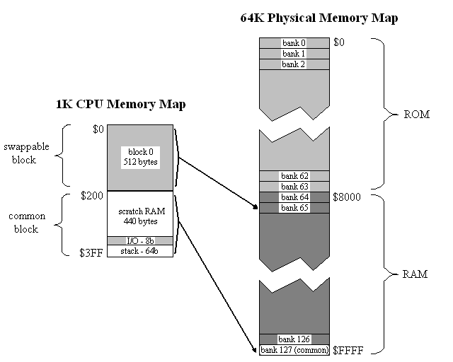
With its 10-bit address bus, the CPU sees 1K of memory. This is divided into two 512-byte blocks. Block 1 contains the stack, I/O ports, and a scratch RAM area. It is the “common” block, and is always present in the CPU’s address space no matter what is happening with bank switching. In contrast, block 0 is a swappable memory area, and can be mapped to any bank in physical memory.
Physical memory is 64K, and is divided equally between ROM and RAM. The 64K physical memory space is partitioned into 128 banks of 512 bytes each. Any bank can be mapped into block 0. Bank 127 is always mapped into block 1, the common block.
The bank select register is part of the memory-mapped I/O ports in common memory. To swap a bank, the CPU only needs to write the new bank number to the appropriate address.
This may all seem pretty simple, but take a minute to consider some of the implications:
- Upon reset, bank 0 is mapped to block 0. That puts 512 bytes of ROM, 440 bytes of RAM, the I/O ports, and the stack all in the CPU’s address space. That’s plenty for many small programs, and means they won’t have to bother about bank switching at all.
- Larger programs (lots of program code) can be accommodated by bank switching code segments in/out of block 0, all operating on common data in block 1.
- Programs operating on large data structures can copy some bank-switching helper code to block 1, then swap additional RAM banks in/out of block 0.
- Arguments can be passed on the stack to ROM helper routines in other banks, because the stack is in common memory.
- All of ROM is addressable, with no holes. This makes storing images, audio samples, and other data in ROM much easier.
- There is no difference in handling between ROM and RAM banks. A program running entirely from RAM works just like one whose code is in ROM.
Failures
While this design seems relatively straightforward, it took me a painfully long time to arrive at it. I went through several days of failed designs before settling on this one.
My first attempt was to divide the 1K space into a 768 byte ROM region and a 256 byte RAM region, reasoning that most programs would have more code than data, and then simply tack the bank select register onto the existing address bus. So A0-A9 came from the CPU, and A10-A17 came from the register. That worked poorly, because it swapped the entire address space at once. With that scheme, there’s no easy way to grow the program code space while sharing the same data, or vice-versa. It also left holes of inaccessible memory within each 1K physical memory bank, and caused the stack to disappear when switching banks. With more tricks some of those shortcomings could be addressed, but it didn’t seem promising.
My second attempt extended the first by disconnecting some of the higher-order RAM address lines. This caused the entirety of RAM to appear several times in the physical address space, at the cost of having less total RAM available. So for example, RAM might be repeated eight times in the physical address space, so that in the 768/256 ROM/RAM partitioning for banks N and N+8, the RAM portion would be the same in the two banks while the ROM portion differed. That provided a way to handle larger programs with lots of code sharing the same data, but not programs working on large sets of data. It also still had the same problems with memory holes. And with the different sizes and fixed locations of the ROM and RAM regions, it would be difficult to bootload a program and run it from RAM in the same way it would normally run from ROM.
I think there was a third, fourth, and fifth idea too, but the details all sort of blur together. They mapped 1K chunks of physical memory into the 1K CPU address space in different ways, combined with a split of the 1K CPU address space into ROM and RAM regions. They all sucked. I went through a lot of pieces of paper.
Eventually I hit on the idea of tying the ROM/RAM select to the bank register, rather than the CPU address. I don’t know why it took me so long to think of that, when it seems obvious now. I devised a scheme with two blocks with a 768/256 split, where either block could be mapped to any 1K bank of physical memory. When mapping a bank to the 768-byte block 0, the upper 256 bytes were inaccessible. And when mapping a bank to the 256-byte block 1, the lower 768 bytes were inaccessible. Yet any byte in a bank was accessible as long as you mapped it to the appropriate block. This wasn’t TOO bad, but was certainly awkward, and it also required two different bank select registers (one for each block).
Finally I went for a long run in the hills near my home. I find that when I’m sitting at my desk, trying to find the solution to something difficult, it never comes. All my good ideas come to me either when I’m driving, in the shower, or out for a run. About three miles in to the run, I thought about a 512/512 split, and realized that if the banks were also 512 bytes, I could fit a whole bank into a block, and eliminate all this weirdness. As I said, it seems obvious now.
There’s one slightly unintuitive aspect to this scheme, which is a result of having 512-byte banks but a 1024-byte address space. The CPU address bus is A0-A9, but A9 is actually not connected to the memory at all! That took me a while to grasp. Instead, A9 is used as a select input to the address decoding logic, and determines whether a memory reference is to block 0 or block 1. It operates the mux that selects either the contents of the bank select register or a fixed value for the upper address lines. The A9 that is actually connected to the memory chips is generated by the decoding logic and is not the CPU’s A9.
Read 3 comments and join the conversation3 Comments so far
Leave a reply. For customer support issues, please use the Customer Support link instead of writing comments.
“It [A9] operates the mux that selects either the contents of the bank select register or a fixed value for the upper address lines.”
If you are using discrete logic, you can eliminate the mux pretty easily. For example with a 74×573 latch as the bank select register you can tie pull-ups to the outputs with a resistor network and the processor’s A9 to the output enable pin. Since the output enable is active low, A9=0 will enable the address of the selected bank. When A9=1, the outputs are in high impedance and the pull-ups will default the address to the last bank.
BTW, that’s a nice figure you’ve drawn to show the memory mapping. What software did you use to create it?
The memory map diagram was drawn in MS Paint. 🙂
Interesting idea about using pull-ups instead of a mux! I’m using a second CPLD for memory decoding and I/O interfaces, not discrete logic, but the same idea could still be used. It would be nice to save a few macrocells in that CPLD too, because space is getting tight.
My concern: with a pull-up, wouldn’t the low-to-high switching time on those address lines be very slow? It’s basically an RC circuit pulling the voltage high. If the rise time were more than about 30-40 ns, it would become the critical path, and force me to lower the CPU’s clock speed. I guess it would depend on the capacitance of the trace and pins, which I wouldn’t know until I make the board. A lower valued pull-up resistor should also help, but use more parasitic power.
MS Paint -> wow! I don’t think I would have the patience.
Yes, there’s a speed/complexity/power trade-off. I guess I had in my mind that this was going to be only running at a few MHz. For high speed and low power your original plan of a multiplexer sounds better.