

Guess the Number
It’s programming time! To verify that Nibbler’s design and instruction set are powerful enough to handle a real program, I sat down to write a simple “guess the number” game. And… (drumroll) it works! I ran the program on the Nibbler simulator, and interacted with it using the simulated pushbuttons. Hint for competitive players: you can always guess the number in at most log2(range) guesses. 🙂
At startup, the program asks the player to press any button. While it waits, it constantly increments a 4-bit counter, incrementing from 0 to 15 and rolling over back to 0. The value of the counter when the player presses the first button determines the secret number he’ll be trying to guess.
Next, the program prompts the player to enter a guess. Pressing the up/down buttons increases/decreases the guess number, and pressing the right button submits the guess. The guess number is converted to text using a crude nibble-to-ASCII conversion routine, which does a byte-wide addition of the number to the character literal ‘0’, performing carry propagation from the low to the high nibble. After submitting a guess, the LCD display changes to “Too high!”, “Too low!”, or “You got it!”, and the player is prompted for a new guess. View the Guess the Number program listing.
While the program runs perfectly on the simulator, there are a few details that probably need to change to make it work on real hardware. Button debouncing code needs to be added, since real buttons don’t cleanly change between their 0 and 1 states, but bounce rapidly between states for a few milliseconds when the button is pressed or released. The LCD initialization and timing code may also be off – I’ll need to verify that on real hardware to be sure.
Program Analysis
The guess the number program assembles to 1135 bytes, or 27% of Nibbler’s program memory. Writing the program was an interesting exercise in coping with the limitations of the CPU’s simple design:
- Registers – Nibbler has just one CPU register: the 4 bit accumulator “A”. Surprisingly, working with only one register didn’t cause many problems, and there were few instances where additional registers would have made a difference.
- Call/Return – The lack of a stack in Nibbler means there’s no call/return mechanism, so no way to call subroutines in the traditional way. This was an annoyance, but I was able to work around it by using a dedicated memory location called
RETURN_ADDRESS, and testing its value at the end of subroutines in order to determine where to jump next.
- Indirect Addressing – All Nibbler memory references use absolute addressing, with no indirect or indexed address modes. This was a bigger annoyance, and working around it led to some ugly code bloat. To get the Nth element from an array of size K, the code must perform K tests of the value of N to determine the correct absolute address. This approach would be impractical in a system using large data structures, but for the types of programs planned for Nibbler, it works OK.
- Program Literals – The biggest headache turned out to be working with arrays of constant data: the character strings like “Press any button”. These had to be copied to data memory one nibble at a time, using LIT and ST instructions, resulting in major code bloat. With this technique, each nibble of constant data requires three bytes of program space. With 4096 bytes of total space, this limits Nibbler programs to a few hundred bytes of strings and other constant data, but that should be enough.
Tool Updates
Along the way, I made a few improvements to the toolchain. The Nibbler assembler gained the ability to do basic math on address labels, such as
ld LCD_BUFFER+1
to load the accumulator from the second nibble of LCD_BUFFER. This proved to be extremely useful, as you can see in the program listing.
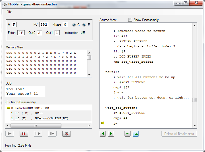
The second major improvement was to the simulator. I grew curious how fast the simulation was running in comparison to the planned clock speed of the real hardware, so I added a simulated MHz status line at the bottom of the simulator window. It turns out that the simulation runs faster than the real thing, averaging about 3 MHz when running on a 2.5 GHz Core i5 computer. Not bad for managed .NET code that was written with no thoughts for performance optimization.
Read 17 comments and join the conversation
17 Comments so far
Leave a reply. For customer support issues, please use the Customer Support link instead of writing comments.
A few Questions to understand the code:
a) what is an _ori / _andi as used in lcd_write-nibble
b) is it realy necersarry to access a (at teh moment) unavailable programm? Wouldn’t it be more useful to use something like ANDI #$F – not realy a NOP, but at least not addressing some hardware that could cause problems in future Versions.
c) Is there a reason (beside programming as used on other CPUs) to store the nibble loaded in lcd_write_buffer to LCD_NIBBLE? After all, the first instruction is to load it again, so just keeping it in A would save 16 instructions (32 Bytes, ~3% of your programm).
Another improvement in programming style would be to use the fact, that neiter LD nor ST does influence the flags.
Looking at the code, I think it would be (as usual) a huge improvement if I’O hardware would offer ‘inteligent’ operations. Like providing some STROBE signal when writing to a port. It would make almost all of lcd_write_buffer obsolete. Outputing a nibble would be reduced to
LD nibble
OUT #PORT_LCD
If now in return the external device can pull a wait line to stop operation until ready again, we would in fact speed up operation by waiting – and reduce code size by a reasonable amount.
Such a wait cycle could be implemented either by just stoping the clock while /WAIT is assigned, or by adding a FF that get set by each OUT and cleared when /WAIT is high. It’s output is routed to the micro programm, and every OUT will result in a stall until the input is cleared. Well, the later one would add the the chipcount and result only in a rather marginal speed gain (due paralell operation of CPU and IO).
A simple /WAIT to stop the clock would not only wlp in IO but also souble as hardware single step solution.
It might be a good idea if CPU design and IO design could get seperated – making an IO_bus of 4 address lines, 4 data (or 8 if uni directional) two strobes (/IOR, /IOW) and said /WAIT signal up as the interface. Otherwise the nibbler might wander too much away from beeing a gernal purpose CPU toward a very specific micro programmed game circuit.
While the solution of using a label compared return technique is well known, on the Nibbler it will again hit the data size barrier – there are only 16 possible return addresses for each subroutine (unless we use two cells) thus it’s not only a bloat, but also a serious restriction in usability.
I can’t realy come up with a different solution, since any handling of data wider than 4 will no only result in multiple cycles (not a big problem, since this could be handled thru microprogramm) but also in several additional chips to route and buffer the address information. It got a lot in common with the indexing issue.
Looking at your code, I did come up with two ways to lessen the cost.
First would be (again) a DJZ A is send thru the ALU to be decremented and a jump is taken if negative (using A=B output). With a DJZ, the return table would shrink to two bytes per resturn, which is at least spacewise similar to what could be archieved by soe return table command. Speedpenalty would be halved. A returntable now looks like:
LD RETURN_LABEL
DJZ next0
DJZ next1
DJZ next2
…
The other improvement is a kind of an indexed/special page jump. Let’s call it SVC P,F wher P is a 4 Bit parameter and F is an 8 bit address. SVC will load A with P and jump to an address in the 0xx Range with xx supplied from the second instruction byte (P). All changes to support this instruction are in the micro programm. Here it is operated almost as with a JMP, except that /loadA is active and a new output signal is connected to the /clr input ot the topmost ‘163 (AFAIR CLR overwrites LOAD).
Also, at least in the case where such output chaining as with the buffers is happening, we can move the overhead of the jump table (for detailed part) back to where it is originated (aka the caller).
With this change the whole output will become evel less than what is now needed to just fill the buffer:
LD #15
ST local_ret ;some local cell, or whatsoever – coudl be like a static stack
LD #OUT1 ;some sort of automatic label generation needed
ST lcd_out_ret ;Again, assembler should help here
OUT1:
SVC #’P’,LCD_OUT1
SVC #’r’,LCD_OUT1
…
OUT1A:
LD local_ret
DJZ OUT1+2
DJZ OUT1+4
DJZ OUT1+6
DJZ OUT1+8
…
; done with out1
…
LCD_OUT1: ; Located somewhere in the first 256 Bytes – either direct, or via a jump there – so 128 SVC routines are possible
OUT #PORT
…
LD lcd_out_ret
DJZ OUT1A
DJZ OUT2A
…
This way we need just 4 bytes for each nibble to be send – barely more then already needed to fill the bufer alone. (A Compare and Skip operation would reduce it to 3 bytes per nibble!)
With a bit playing on the feature to place routines in the first 256 Bytes, furter improvement could be reached.
Still, no sub routines, but more compact handling for an often needed case.
Hans, you’re full of interesting ideas! I feel bad that I haven’t used any of them yet. But going back to the original Nibbler goals, I really want this to be the simplest possible working example of a 7400 CPU, so I can use it as an example for how to get started. Thinking more about what “simplest possible” means, I decided it doesn’t necessarily mean lowest chip count, but it means the architectural diagram (http://www.bigmessowires.com/nibbler-architecture-v3.png) should be as simple as possible. That means the CPU will probably be cumbersome to write programs for, and not very efficient, but that’s an OK trade-off for my purposes here. Introducing wait states and other improvements would definitely shrink the program size and probably speed things up, but isn’t really in keeping with the goal of maximum simplicity.
> what is an _ori / _andi as used in lcd_write-nibble
These are synthetic instructions, as described in a previous post. So _ori #X assembles to:
nori #X
nori #0
> is it realy necersarry to access a (at teh moment) unavailable programm? Wouldn’t it be more useful to use something like ANDI #$F – not realy a NOP
Unfortunately there’s no instruction that functions as a true NOP. ANDI #$F is a fine alternative if you don’t mind altering the ALU flags.
> Is there a reason (beside programming as used on other CPUs) to store the nibble loaded in lcd_write_buffer to LCD_NIBBLE? After all, the first instruction is to load it again, so just keeping it in A would save 16 instructions
Good idea.
> First would be (again) a DJZ A is send thru the ALU to be decremented and a jump is taken if negative (using A=B output)
I like this idea, but I’m not clear how you mean to implement it with the current hardware design. I’m not sure how the A=B output could be used, since the B input comes from the data bus. From your example, it looks like the jump is supposed to be taken if A is zero *before* the decrement rather than after, so it’s really a JZD rather than a DJZ. But even that’s not possible with the current hardware, as far as I can see.
Thanks for the ideas!
No harm done – i’m just quite exited about this project. In fact, I wait already for some ‘pleste STFU’ reply :))
a) Simplicity:
I think we’re not far from each here. To me simplicity does also mean not to ignore gains possible. Of course a limited design like here will not be as luxurious as others known (although, I don’t realy would go there – each and every CPU I have met so far is cumbersome in some way – especially when you programm against it’s structure). How complex you diagram is, depends quite on the level of abstraction.
a1) Your Diagram already does not show all controll lines, so SVC, DJZ and /wait will not add complexity (SCNR 🙂 I try to restrict myself already to ideas not adding (much) hardware at all.
a2) /wait is ment to be just filter CLK away, so it’s just an AND Gate.
b) yeah, I could have guessed that myself – Didn’t think about only offering NOR when reading 🙂
c) When moving toward RISC, a true NOP would be available for free (operation C=A)
d) Programming: I got a feeling (no solution yet) that we could bring it on if we find a way to eliminate the output buffer. Such inbetween buffering is common in todays architectures, but not realy efficient. (no offense intended, but I have a feeling as if you’re somewhat stuck in well known traces)
e) DJZ
A=B is in reality not a comparsion of bot inputs, but rather just anding together all 4 output signals, so a value of $F will set A=B. Now operation $F of a ‘181 (I have to look for my databook soon, I’m writing so much without doublechecking here) is C=A-1 – thus offering exactly the operation we want – decrementing A and signaling wenn going below zero. This is the case when A holds zero. Unless I’m completly off track, just what we want.
It’s quite long ago (>30yrs) ago since I did a real ‘181 based design (read something that got soldered afterwards). So memory might be a bit blury. Fun fact about back then: If possible things like incrementing the PC was rather done by microcode and using the ‘181. This way ‘173 could be used instead of the more expensive ‘163
In a static view, whenever the A inputs are all zero and function is arithmetic $F, A=B will go active. I have to go thru your schematic and see if it is Zero before or after – important is here when the load of the 173 takes place. Not that it would matter a lot for the funcionallity at all. Programming should take place to correct such behaviour – Saving half the instruction on a switch table is making a lot good for adjusting +/-1 before 🙂
Again, I need to look for my books … somewhere in my Kack Pile De Luxe.
I have a real desire to make this on an FPGA. I won’t though, I have 1000 other better things to do 🙂
Some more thoughts on your suggestions, Hans:
1. I eliminated LCD_NIBBLE, and passed the nibble to write in the accumulator instead. This saved 47 bytes of program space.
2. Wow, you’re right that the ‘181 ALU’s A=B output doesn’t actually test if A=B, but if the result is $F. My simulator and microcode for the CMP instruction are wrong… I’ll need to fix.
3. I don’t think A=B could be used to implement a DJZ instruction in the way you suggest. A=B is an output of the current microcode step, so it can’t also be an input into that same step without creating a combinatorial loop, and making two trips through the microcode ROM during the same clock cycle. It could be stored in the E bit of the flags regsiter, but then DJZ would need three clock cycles to execute: 1) fetch 2) decrement 3) conditional jump.
A similar idea that I think could be done with the current hardware is a JNCD instruction – jump if no carry, and decrement. It would jump if the carry bit was not set, and would decrement the accumulator regardless of whether the jump was taken. The semantics would be a little strange, but I think it would work.
addi #-1 ; first decrement is manual, to set the C flag
jncd BRANCH0
jncd BRANCH1
jncd BRANCH2
…
I just realized why the ‘181 has all those references to “active low mode” in the data sheet. If I invert the inputs to the ALU, then the outputs will also be inverted, and the A=B output (which is true when the 4-bit result is 1111) will become a Zero flag. That’s a lot more useful than an Equal flag. I think I can do this almost for free, by replacing existing bus drivers with inverting drivers, and changing the microcode. More soon…
And back for a JZD 🙂
While at the microcode, maybe also check for the Supervisor jump (SVC) it’ll save 1/3rd code wherever we have a LD imm/JMP combination – important the way subprogramms are done.
When changing the data path to low active, only the input/output lines need to be changed. The ALU result driver must stay uninverted. Also the immediate driver can stay uninverted, just have the assembler invert all immediate values when generating code.
Thinking of it, no hardware has to be changed at all. Just have the assembler code the immediate values the right way – and define the port constants accordingly 🙂
Almost, but not changing any hardware would cause data written to OUT registers to be active low, and data read from IN registers to be read incorrectly.
Sorry, I’m not clear what the advantage of SVC would be. The current method has a marginal cost of 3 program bytes for each extra nibble written (a LIT and a ST). Even assuming a DJZ (or JZD) instruction exists, the SVC method has a marginal cost of 4 program bytes for each extra nibble written (a SVC and a DJZ). There would be some reduction in the fixed cost with SVC, but it would be outweighed by the extra marginal cost for any program that writes more than a few dozen nibbles.
a) active low logic
You’re right, data written or read from in/out have to be handled apropriate. But this only means to take care when defining the constands used – and for I/O hardware to be designed the same way. In programming it means replacing and by or and vice versa. These instructions are syntesized anyway, so where’s the deal?
b) SVC
SVC is not connected with JZD in any way. The idea of SVC is to combind a load imm instruction with a jump to save one instruction, since such a combination will be rather often encounteres. Most basic whenever you jump into a subroutine. Right now you need to go
LD #returnindex
ST _some_ global_save_location
JMP subroutine
5 bytes and 3 cycles per invoke and the knowledge of a global address. With
SVC #imm,trap
a subroutine call will only take two bytes of ptogram code and a single cycle when invoked. In most cases the entry of the subroutine will store A into a local (known) variable for later use. But thats only two bytes and a single cycle – so even with a single use of a subroutine 1 byte and one cycle is saved. Each further call will save 3 bytes and two cycles. The number guessing code with 15 ‘next’ lables used would be reduced by 43 bytes (and 29 cycles). Looking thru the source, one might find more to save.
In my example I tried to push the savings by JZD and SVC to a maximum (And I feel that using a buffer is a less than optimal solution, since it requires at least twice the usage of an indexed address). Maybe I should have seperated the descriptions
When counting the overhead, you also need to see the saved amount within the lcd_write_buffer function – after all, it’s 9 bytes selection code per buffer nibble (total 160 bytes *1). It needs quite a bunch of output calls ( like more than 160 🙂 to be spend on the call side.
*1 – BTW, there’s another little programmign quirk – for one, in your CMPI ladder you do not realy have to compare for #15 – after all, having compared for everything from #0 to #14, there is no other value possible. But even if you decide to do so, it would be a good idea to have a lable where the JNE + should jump to. One of the little quirks when local lables are used outside of dedicated macros 🙂
P.S.: Drop all ‘NOPs’ but one and increase the loopcounter to 13 – saving 6 bytes :)) SCNR – I think I’m already looking way too long at this code 🙂
*Oops*
Forget all my musings about new operations – I just realized I got the Nibbler-B (Nibbler with a B register) in my mind all the time – there is no code space in the original definition to add JZD or SVC.
Sorry for pushing this.
No worries, those instructions could still be added in place of JNC and JNZ.
I agree JZD probably makes sense to include, I’m just uncomfortable with the idea of a decrement and jump instruction where the jump is not dependent on the decrement. It’s unintuitive. Maybe a different name like DJN (decrement and jump if negative) would help, although that’s not quite accurate.
I still don’t see how the proposed SVC instruction would make programs smaller. I agree that in the case of passing a single nibble constant to a subroutine, SVC would save one byte vs a LIT followed by a JMP. But in the case of sending long text strings to the LCD, the buffered write method has a smaller incremental cost for each nibble written. Here are two sample programs that demonstrate this:
http://www.bigmessowires.com/nibbler-sample1.asm
http://www.bigmessowires.com/nibbler-sample2.asm
The buffered method has a fixed cost of 148 bytes, and an incremental cost of 59 bytes per 16 nibbles written.
The SVC method has a fixed cost of 63 bytes, and an incremental cost of 91 bytes per 16 nibbles written.
If a DJZ instruction existed, it would lower the SVC’s method’s incremental cost to 76 bytes per 16 nibbles written. After writing five sets of 16 nibbles, the higher incremental cost would surpass the fixed savings. So any program writing more than 5 * 16 = 80 nibbles (40 letters) using the SVC method would be larger than with the buffered method.
You’re right, JZD looks strange when seen from the usual instruction sets, but synthesizing all logic instructions is at least as strange. I think we are exploring ways of maximal productivity from minimal hardware, so unusual (I prefer this ofer the not realy fitin term of unintuitive) instructions are the way to make most of it’s talents.
What I do not realy understand why you’re so fixed on the full figured example. Please take another look at my example (9/4 6.37PM) – SVC does not need to be used to replace the buffer – allone by improving the jump to the print routine it would save about 4% of your code – and way more in larger programms.
And yes, when your buffer might be less code if you always use it to the max (still quite slow) – then again, most programs will not always output 8 Bytes at once, but usually less (*1), making it less efficient (but slow).
*1 – here is BTW another simple emprovement to the code, you got two string outputs starting with “Too_” spliting this into a common output and two shorter might save code).
With all the rather huge overhead for subroutines, some kind of subroutine support in hardware might be a good idea. My thoughts runn arround a solution with a single level JMP register – allowing one level of subroutine. It’s a bit like most very early computers. Most notably maybe the Mailüfters (still an open issue it it hace been the first fully transistorized computer or the 2002), which featured a simgle link register that would be writen to by a (special) jump and could be read (and afterwards stored to PC).
I see three possible solution:
a) A register able to hold a single address, only loaded by a (special) JMP instruction. Later on the content can be used to reload the PC. No other operations are possible. Requires two instructions
b) Some kind of a ‘Jump-Port’ – 4 port adresses used to handle a return address. Port 0..2 can be writen to for holding an address, port 4 issues a strobe to load the PC with the content of port 0..2. No instruction set change is required.
c) A combination of both where every (unconditional) JMP copies the actual programm address into port 0..2, which can also be read from.
Pro/Con
a)
+ no additional operations needed
+ fastes possible execution
+ 1 level already offers a great improvement
– requires two opcodes (or one with a reserved suboperation)
– no address calculation is possible
b)
+ full software control
+ calculated jumps are possible
+ could be used for dynamic ROM access (reading data tables, output strings, etc.)
+ variable ‘return’ address (chaining etc).
+ combination of above (returning after the end of an output string)
– jumps need to be prepared by software
– 6 (1 byte) instructions to prepare a subroutine or calculated jump)
c)
+ no preperation needed
+ simple execution when no parameters are handled
– rather ‘huge’ hardware effort
– address manipulation needs several instructions.
Well, I’m running in circles here. I want to keep it simple, but I see a real need.
I see what you mean now. In your example, I thought SVC #imm,trap was passing a parameter, but it’s actually passing the return address.
I like your return address ideas, but I don’t find the current method of jump tables to be so bad for my Nibbler’s purpose. Probably I will do another 7400 CPU later where the goal is efficiency instead of design simplicity, and do something like what you’re suggesting for the return address.
If I added two new instructions in place of JNZ and JNC, they would probably be:
JZD $address (or DJN or whatever it’s named) – This would help shrink jump tables and indexed lookup tables. Would have a fixed savings of about 30 bytes in the guess-the-number program.
STI #X,$address – Store immediate. This would reduce the code for every nibble written to the buffer from 3 bytes to 2, saving about 200 bytes in the guess-the-number program, or more in programs with more text. But it would require reducing the RAM address size to 8 bits (256 bytes of RAM), or adding mux hardware to conditionally set the high bits of the address from either the normal source, or a constant zero.
Well, for the Nibbler design, there is no difference between return address (identifier) and a parameter – after all, it’s never a difference, on ‘standard’ CPUs a call is just a jump with an implied passing of another argument (return address), and a RET is just a POP/JMP combination.
LITI (if you call the LD #imm LIT , then this is kind of an extendet version) is a good choice. It saves a whole instruction and 33% code. Not just for the buffer, but wherever a RAM cell needs to be initialized. it is a good choice. But not realy a reason to reduce RAM to 256 nibbles. Rather try to view the first 256 nibbles as a kind of zero page (like on a 6502) where a special shortcut instruction for initialization is availabe.
Now, on the other hand, if we restrict a RAM address to 8 Bit, we could use the 4 Bit field for some other functionality … I have to think about it.
Hmm, Different address size – it makes me think about the TI TMS1000 again. That CPU was available with a ROM size of 1 and 2 k (8 Bit words) and 64 or 128 RAM cells (4 Bit wide). So with 4K Words (8 Bit) of ROM and 256 Words (4 Bit) of RAM we should (at first sight) be able to do anything the TMS1000 could do – and that has been a lot, like games from MB’s Senso to Parker’s Electronic Mastermind, Alarm Clocks to Microwaves. I think I read that at over the Time TI alone produced more than 6000 different ROM versions, not counting second source suppliers.
But the TMS 1000 was a bit weired – it had an Y register (a bit like our B) that could be used as ALU input and as a target instead of A, but it’s content could only be used for further calculations, or to address memory, while A can be stored to RAM. RAM addressing is done via Y plus a page number from another register, which can be loaded by addressing instructions (it supplies only 2 or 3 bits, depending on RAM size.
Oh, yes, ROM was also paged. There is a 4 bit page register addressing a ROM page of 32 bytes (6 bit). PC was also only 6 bit and wraping every 32 instructions 🙂 Every instruction was 8 Bits (possible since Addresing was always done via X:Y). Intstructions itself where QUITE weired – your single NOR is simple compared to the weiredness the TMS1000 offered – even more, since some instruction bits coudl be used with PLA like logic to modify instructions to handle the programmable I/O system. The chip was a realy strage combination of programmable logic and a CPU – but due this nature awesome flexible. Like the total oposite of todays simple symetric CPUs.
In fact, the nibbler is way more like a modern flat addressing othogenal CPU than a classic 4 bit beast.
Oh, and the TMS1000 had a single subprogramm stack – it could hold one 6 Bit return address – so subroutines had to be within the same 32 Bytes :)) I guess, for performance comparsion the TMS1000 might be a tough competition – with just aplying todays lazy and uncreative programming it will be next to impossible to beat.