

Dirty PCBs Review
Today’s electronics hobbyists are blessed with many options for custom PCB manufacturing, like Seeed, Elecrow, and OSH Park. For around $1 to $2 per board, depending on size and quantity, these vendors will turn your EAGLE or KiCad or other Gerber files into shiny new PCBs. I’ve used all three in the past, but my go-to vendor for most things is Seeed.
Dirty PCBs is a newer entry in this space, but it’s affiliated with Dangerous Prototypes, who are long-time members of the hobbyist electronics community. A few years ago Ian Lesnet moved himself and the company to Shenzhen, China, and Dirty PCBs is sort of a matchmaking service between Shenzhen PCB manufacturers and hackers around the world. For a recent PCB purchase of 20 boards, I decided to give them a try.
Saving Pennies
The main attraction of Dirty PCBs is the price. Even among other cut-rate PCB manufacturers, it stands out as the cut-ratest. Any color PCB is available for the same cost, whereas most manufacturers charge extra for colors other than green. Slow-boat shipping is free worldwide, and the faster shipping options tend to be cheaper than at the competition. For my order of 20 red PCBs, 10×10 cm size, shipped by DHL China, here’s how Dirty PCBs compared to Seeed:
10×10 cm PCB @ qty 20 = $57.43
Red soldermask = $10.00
DHL shipping to USA = $24.71
TOTAL = $92.14
Dirty PCBs
10×10 cm PCB @ qty 20 = $50.00
Red soldermask = $0.00
DHL shipping to USA = $15.00
TOTAL = $65.00
Dirty PCBs also uses a constant price per board as you increase the quantity, or offers a small discount for larger quantities, as you would typically expect. Seeed has the bizarre habit of offering a negative “discount” for higher quantities. E.g. with Seeed it’s sometimes cheaper to buy 10 boards twice than to buy 20 boards.
Ordering
My biggest gripe with Dirty PCBs is the website itself and the way it’s marketed. The site’s tagline says “No bull, just crappy PCBs.” I suspect I’m in the minority, but I just don’t appreciate the joke here. Call it basic, no-frills, or rock-bottom if you like, but please don’t tell me I’m paying money for something that’s intentionally crappy. Especially when, if you read the specs and the terms, it’s not crappy at all. Yet I’m somehow left with a mental picture of a sloppy, careless, and all-around half-assed manufacturing process. I don’t think it’s accurate, but that’s the image it paints in my mind.
To be fair this attitude is intentional, and can be traced to the “accidental” launch of the Dirty PCBs service. As Ian tells it, he never meant to launch a PCB service, but simply hacked together some scripts for the convenience of his friends. That unofficial “for friends” service became unexpectedly popular, and Dirty PCBs was born. Ian’s said in the past that the service doesn’t really make any profit, so his tolerance for whiners and time-wasters is low. To quote the About page:
This site was intended for friends and not the public. We’ll process your boards, but we only make about 30 cents per order. We really don’t care if you want to take your business somewhere else, and it’s not worth our time to deal with stupid questions or asshats. Paypal fee reversals, annoying emails and the like will get you banned from the site.
Fair enough, and +1 for use of the word “flippant”. The actual ordering process was simple, except for a mistake I made when uploading the Gerber files. The upload button doesn’t mention what file format it expected (I later found this information on the About page), so I uploaded a zip archive of the same Gerbers I would normally send to Seeed. It appeared to work, and I went through the entire checkout and payment process, only to be informed after I’d paid that no board outline file was found. This was because my Gerbers had different filename extensions than Dirty PCBs was expecting. After renaming the files and uploading a new zip archive, all was well.
Delivery
My order was placed on Thursday afternoon, and the finished PCBs were in my mailbox on the following Wednesday afternoon. Six days! That is crazy fast. Maybe I just got lucky and hit the manufacturing cycle at the perfect time, but that’s more than twice as fast as any other PCB order I’ve ever made in China or the USA.
Inside the box was an unexpected surprise – 23 PCBs instead of 20. I know the Dirty PCB’s proto-pack is “about 10” and often 11 or 12, but I didn’t realize they did a similar thing for larger orders. Presumably they make 10% extra in case some PCBs fail the e-test, then mail you all the boards that passed testing. So hey, three extra free boards. Thanks!
Inspecting the Boards
Now for the key question: were the boards any good? From my inspection, I’d say mostly yes. I spent a long time examining the boards under 10x magnification, and comparing them to my original EAGLE files, and to the Gerbers using gerbv. Probably I’ve never examined any PCB quite so intensely, and some of the issues mentioned below may be typical of other discount PCB manufacturers too. For the money paid, I’m not complaining, but for completeness I’ve catalogued the good and the not-so-good.
The Good
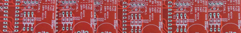
First and foremost, my sample PCB worked great once I populated the components and put everything together. This is about the only thing that really matters in the big view, and it means there were no accidental shorts or breaks in the PCB traces. Of course I hadn’t really expected any problems there, since Dirty PCBs advertises a minimum 5 mil trace/space size, but I only went down to 8 mil and was nowhere near the limit.
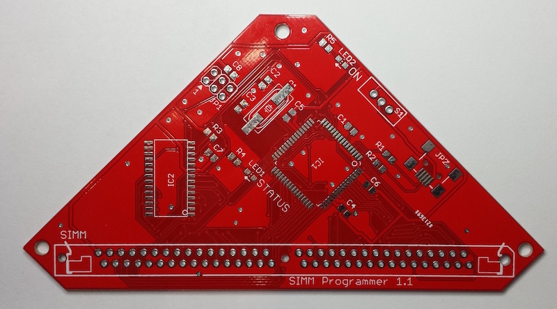
My board is a rather funky hexagon shape, or a triangle with clipped corners if you prefer. There were no problems routing this non-standard board outline.
When examined under magnification, all the drill holes appeared nicely centered in the vias and pads. The edges of traces and planes appeared clean and crisp. Silkscreen was sharp and nicely legible. The soldermask was a nice bright red color, and tented vias were actually tented.
The Not-So-Good
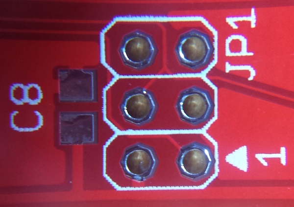
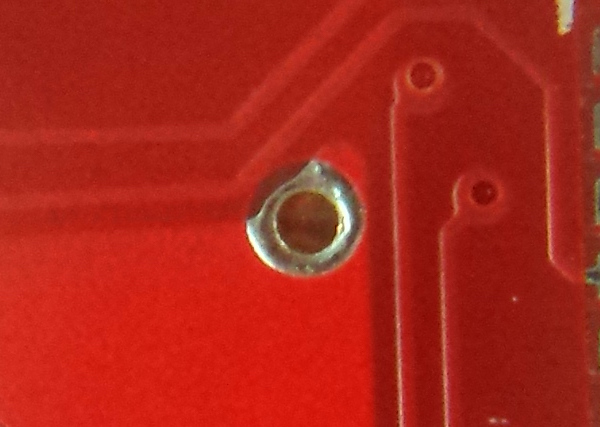
One small gripe: the silkscreen layer was slightly offset from the copper layers and drill holes, as you can see in the photo below. The silkscreen outline for this AVR ISP footprint isn’t centered around the pads. This doesn’t matter much, but it may bother you if you’re a stickler for little details.
One bigger gripe, that I’m still not sure is my fault or Dirty PCBs’ fault: some of the extra-large vias appear either larger than intended, or not in the right place – it’s hard to be sure which. Here’s an example of a large untented via that connects ground planes on the top and bottom of the board. In the photo, notice how the edge of the drill hole is almost exactly in line with the edge of the ground plane (which is partly obscured by the silkscreen line)? And the plating around the drill hole actually extends beyond the ground plane, bowing outwards slightly into the gap between the ground plane and the neighboring trace? And the stop area (the area without soldermask) extends nearly all the way to that neighboring trace?
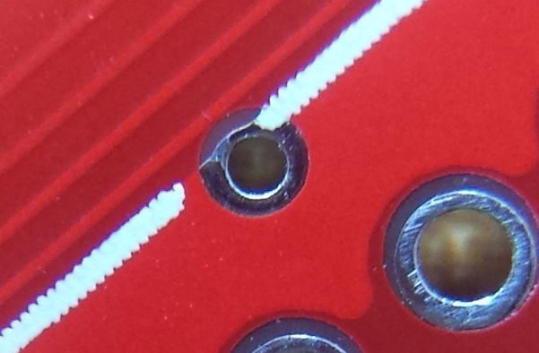
Here’s the same region viewed in EAGLE, with the silkscreen hidden. Notice that the drill hole comes well short of the ground plane’s edge, the plating around the hole doesn’t extend beyond the edge, and the stop area only extends maybe one-third of the way into the gap between the ground plane and the neighboring trace.
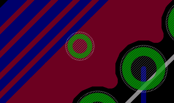
And here’s the same region once more, looking at the actual Gerber files with gerbv. The top copper layer is magenta, drill holes are lavender, and the stop mask is gray. Maybe the Easter Bunny chose this color scheme. Where layers overlap you’ll see additive coloring. There’s no separate color for the plating around the hole here, since both the plating and the ground plane are just part of the top copper layer. It almost looks like Dirty PCBs interpreted the stop mask layer (gerber.GTS) as an additional top copper layer, than generated its own stop mask around that.
Another possibility jumps to mind as I type this: I used a non-standard drill size for those extra-large vias of 0.02362205 inches – not sure how that happened. I wonder if DirtyPCBs rounded up to the next larger drill size, then automatically enlarged the copper area and stop mask to compensate. The through-hole pads in these pictures use a 0.040 inch drill, so the ratio of the hole sizes should be 0.02362205 / 0.040 = about 0.59. But measuring the actual hole size ratio observed in the PCB photo, it’s about 0.62. So those via holes are about 4.7% larger than they were intended to be, if my figuring is correct.

Here’s another example of the same issue. This via bulges outward slightly from the top-left of the ground plane, and the stop area extends all the way to the neighboring trace. But in the source file, the via’s drill hole and plated area are both completely within the boundaries of the ground plane, and the stop area only extends about a quarter of the way to the neighboring trace.
Overall Rating
As an overall rating, I’m giving Dirty PCBs a thumbs-up. They were cheap, super fast, sent me extra boards, and the boards worked. I’m not sure I’d trust them yet with a design that goes all the way to the 5 mil limit, but it’s probably best to avoid that limit anyway. I wish they’d change the name or at least the tagline, but that’s just me. I expect I’ll use Dirty PCBs again, and will report how it goes. Thanks for reading!
Read 6 comments and join the conversation6 Comments so far
Leave a reply. For customer support issues, please use the Customer Support link instead of writing comments.
I totally agree with the tag-line. I was actually waiting to read a review like this before even trusting it for a one-off prototype, but thanks for the post. Now knowing the limitations, I see no reason not to give them a shot.
Cheers.
So I dunno if these guys are still under the same management but I had a weiiird experience trying to order. I put in a 4 layer design and verified it with their layer report tool, got a very good and reasonable looking price quote, and since it offered a steel stencil for a very reasonable additional charge, I went for that too.
Shortly thereafter I started getting messages from “Bernadette” asking for all kinds of extra fees. First it was “You need to pay $35 extra for a DHL Remote Area Delivery fee” (I live in San Francisco, I checked DHL’s site, they do not require any remote delivery fee for my address.)
Then I got another one saying there’s a $20 extra fee for the stencil because “our system is not yet automated correctly for calculating customized 4 layer board with steel stencil.”
Then I got yet another one saying there’s a $250 (!) extra fee because “your design is 6 layers” (It’s not, their own layer report shows exactly two internal layers plus top and bottom.)
I finally asked them to just cancel the order because it was starting to sound scammy. They’ve already billed some of this to my credit card so I hope I don’t have to fight over it.
Bologna, there is no way they are doing it at-cost (as they suggest). Prices aren’t great! Both PCB manufacturers that I already use are significantly cheaper, and these companies strive for quality. Why would I pay more for potentially crappy boards? I don’t have time for them to screw up the order and then refund me. The whole site is a ploy to convince would-be buyers that they must really be getting a bargain, when they’re not. The only thing that I like is the timeframe, if it’s truly the case. I’m usually waiting 4-6 weeks.
Recently, i found a company called jlcpcb. It’s very cheap
10pcs boards. 1.2mm thick, 1-OZ copper, 6/6-mil outer (0.1525mm) just cost $2
https://jlcpcb.com/
Very useful article. Or you can try more PCB manufacturer, such as https://www.wellpcb.com
Very realistic PCB review. Very welcome to order our PCB prototype, and we provide PCB prototype and assembly. https://www.ourpcb.com