

Yellowstone Arrgh

I’m still struggling with these Yellowstone card electrical problems, but getting nowhere. Very frustrating. I’ve focused my attention on the large amount of overshoot on the data bus, and the power supply fluctuations, under the theory that minimizing those will eliminate all the functional glitches and failures I’ve experienced.
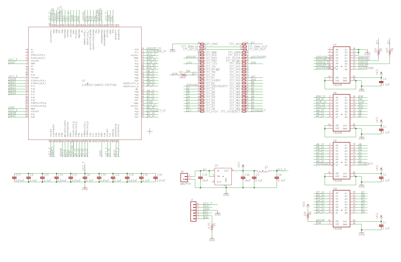
The FPGA has eight bidirectional pins that are connected to one side of a 74LVC245 buffer. The other side is connected to the data bus. The buffer’s direction is controlled directly from the CPU’s R/W signal, and the buffer’s output enable is controlled by FPGA logic. The FPGA pins direction are controlled by separate FPGA logic. See the schematic here.
The image above shows the moment when the card starts to drive a value on the data bus.
Channel 1 (yellow) is a copy of the slot’s /IOSELECT signal, passed through the FPGA. When it goes low, it means the Apple II wants the card to drive the bus.
Channel 2 (light blue) shows D0 on the data bus. Notice how it climbs from 0 to 2V, retreats back to near 0, shoots up to 4.6V (a good trick for a 3.3V chip), and finally settles at 3.3V? Yuck.
Channel 3 (pink) is an internal active-high debug signal from the FPGA that shows when it’s outputting a value for the 74LVC245 buffer. This is a sanity check on what’s happening.
Channel 4 (dark blue) shows the Yellowstone card’s ground, with respect to the Apple II system ground. Note the scale: it doesn’t look like much, but there’s almost 1V of peak-to-peak ground noise.
Besides the data bus overshoot, there’s also something odd with /IOSELECT on channel 1. Because there’s no convenient place for me to physically probe the actual /IOSELECT signal, I used an FPGA debug output pin to mirror /IOSELECT and capture it with the scope. The result should look identical to the actual /IOSELECT, except shifted to 3.3V logic levels rather than 5V, and with a few nanoseconds of extra delay. But why is there 1V of undershoot on the scope when /IOSELECT first goes low? The scope is capturing a debug output that’s just a two-inch trace on the Yellowstone card, with no other load except the scope probe. I was not expecting to see any undershoot or overshoot on these debug signals, and the channel 3 (pink) debug signal doesn’t show any.
As bad as that scope trace looks, this one looks worse:

This looks like some kind of glitch, because the FPGA is only outputting for about 60ns, but a normal output lasts about 500ns. /IOSELECT starts to fall, but then goes back up, and shoots up to 5.0V (remember this is an output from a 3.3V chip). The data bus voltage spikes to 6.6V, and the Yellowstone ground reaches 2.0V relative to Apple II ground. Arrgh!
In an effort to troubleshoot this glitch further, I switched channel 2 (light blue) to show the direction of the Apple II motherboard’s data bus buffer, which should (I think) simply be the CPU’s R/W signal. This was the result:

It appears that the glitch occurs just before the end of a CPU write, when the direction switches from low to high. Assuming that’s the CPU R/W signal, that means the glitch starts during a time when R/W is 0, which should be impossible. Here’s the Verilog equation for the channel 3 (pink) signal:
assign isOutputting = (rw && ~_romoe);
If R/W is zero, then isOutputting must also be zero, but from the scope trace it’s obvious that’s false. There’s something happening here that I don’t understand. Maybe the Apple II motherboard’s data bus buffer direction isn’t driven from the CPU’s R/W, but from some other buffered or computed signal.
When I rearranged some things in an attempt to investigate the glitch further, it disappeared. I was never able to find an explanation.
Head Scratching
There are so many strange unexplained problems, it’s a miracle that the card actually works most of the time!
So what causes big overshoots and supply fluctuations? I can think of a few possibilities:
1. 3.3V voltage regulator can’t meet the instantaneous demand for current
2. Insufficient bypass capacitors on the card
3. 5V and GND connections from the card to the slot are too wimpy, and can’t carry enough current without significant resistive loss
4. Impedance mismatch on the data bus, signal reflections, etc.
Considering each of these in turn:
1. There’s a 300 mV LDO on the card, which I’ve calculated should be enough for the average demand. Brief spikes in demand should be satisfied by the capacitors. What’s the behavior of a typical LDO when it’s overtaxed? Does the regulated voltage drop, or does ground get pulled up, or both? If I make another revision of the Yellowstone board, I’ll substitute a larger regulator just to rule out this possibility.
2. My intuition pointed to this explanation first, but it hasn’t been confirmed by experiments. You can see all the bypass capacitors in the schematic: at least one 0.1 uF ceramic cap for the power supply on each chip, plus others recommended by the FPGA and LDO datasheets. I tried jury-rigging additional capacitors at various points on the board, but they didn’t make an observable difference in the signals as viewed on the scope. And even if this were the problem, I could imagine it causing the overshoot seen on the databus, but I can’t see how it would cause Yellowstone’s ground to rise to 2.0V relative to Apple II ground.
3. I tried connecting some extra jumper wires from ground points on the card to ground points on the Apple II motherboard. It didn’t make an observable difference in the signals as viewed on the scope. But maybe 5V has a problem?
4. An impedance mismatch could be part of the problem, but what would I do about it? The Apple II bus can contain anywhere from zero to six other cards of assorted types, so it’s not clear what impedance I should try to match. And all the vintage 1980’s cards I’ve observed don’t appear to have any termination resistors or other obvious impedance matching circuitry – they just connect a 74LS245 or similar buffer chip directly to the bus.
For clarity, I don’t think Yellowstone’s use of a 3.3V 74LVC245 is a problem, at least not in the way suggested by some commenters. Yes, this chip can only drive to 3.3V, but that’s plenty high enough to register as a logical high for the 74LS series logic used elsewhere in the Apple II. And the scope traces clearly show that the data bus voltages are high enough. If the 74LVC245 is causing a problem, it must be some less-obvious mechanism like coupling noise to the 3.3V supply, or maybe a too-fast slew rate.
I’ve pounded my head long enough, and am running out of ideas. Debugging is hugely impeded by the absence of any place to physically probe many of the bus signals, and by a scope with only four analog channels. The scope also has a 70 MHz bandwidth, which might be a factor. I feel too much like I’m scratching randomly in the dark, rather than making systematic progress towards narrowing down the causes of the problems.
My temptation is to design a new revision of the card, and include some speculative changes that might help. I could substitute a beefier LDO, add more capacitors, make the power connections extra-robust, and include additional debug headers for probing bus signals. It can’t hurt, but realistically it probably won’t help either. I could also try adding some termination resistors, but that just seems wrong somehow, given that no other Apple II cards appear to use them.
Electronics can be hard. In the 10 years I’ve been writing this blog, I’ve never encountered a problem that had me so completely stalled as this one.
Read 16 comments and join the conversation16 Comments so far
Leave a reply. For customer support issues, please use the Customer Support link instead of writing comments.
The rise time of your 74LVC245A is about twice as fast as the 74LS chips. With a long bus, that fast(er) edge could definitely give you reflection issues. As someone proposed in the last post, some small series resistors should clean that up. Value shouldn’t be too critical – I think 33 ohms was suggested.
Double-check the ESR of the output capacitor on the LDO against what the data sheet recommends. A mismatch (too much or too little) there could give you oscillation in the output. I’m pretty sure that higher loads exacerbate that.
Would series resistors also slow down the edge times for received signals on the bus? Those are coming from a 74LS buffer and are already “slow”, so I don’t necessarily want to make them slower. Perhaps this is a reason to try substituting one of the dual supply buffers that were suggested earlier, like the 74LVC8T245, if their edges are slower.
On the LDO there’s a 10uF X5R ceramic input capacitor, and 10uF X5R and 0.1uF X7R ceramic output capacitors. The LDO datasheet is here: http://ww1.microchip.com/downloads/en/DeviceDoc/MIC550X.pdf For input it says:
“An input capacitor of 1μF is required from the input to ground to provide stability. Low-ESR ceramic capacitors provide optimal performance at a minimum of space. Additional high-frequency capacitors, such as small-valued NPO dielectric-type capacitors, help filter out high-frequency noise and are good practice in any RF-based circuit. X5R or X7R dielectrics are recommended for the input capacitor.”
I interpreted “1uF” to mean “at least 1uF”, but maybe that’s wrong? I used 10uF. For output the datasheet says:
“The MIC5501/2/3/4 requires an output capacitor of 1μF or greater to maintain stability. The design is optimized for use with low-ESR ceramic chip capacitors. High ESR capacitors are not recommended because they may cause high-frequency oscillation. The output capacitor can be increased, but performance has been optimized for a 1μF ceramic output capacitor and does not improve significantly with larger capacitance. X7R/X5R dielectric-type ceramic capacitors are recommended because of their temperature performance.”
I’m sorry if this is an obvious thing that I’m just missing this morning… but what is L1 doing?
Your comment “shoots up to 4.6V (a good trick for a 3.3V chip)” makes me wonder where the extra voltage is coming from… and there’s an inductor, right there, which would be my first suspect. Is it possible that L1 is causing a brief overvoltage of VCC or VCC_F? Have you measured the output voltage on the 20ns timescale alongside the weird logic voltages?
At first glance I thought you were using a switching regulator, but I didn’t see a feedback pin… so now I’m wondering if you’re somehow getting an accidental intermittent boost topology switcher out of your linear regulator, depending on the load on each side of the inductor at any given moment. Maybe you need a diode somewhere to keep the back-EMF from the inductor under control?
My second guess would be something related to board layout; maybe some board layout issue is giving enough inductance to cause a voltage spike? Are any of the logic lines running near that inductor?
Good question. L1 is a ferrite bead, it separates the 3.3V VCC supply from what I called VCC_F on the schematic: the FPGA’s supply. This is the configuration that was recommended by the FPGA datasheet. The voltages I’ve measured on the scope were all from VCC and GND, as there’s no place to attach a probe for VCC_F. I had the same suspicion you did about L1, and meant to try a test with it removed/shorted, but I forgot. No logic lines run near L1.
I don’t understand your comment about the regulator, sorry. As you can see in the datasheet, there’s no feedback pin. It’s just VIN, VOUT, GND, and an optional enable pin.
I removed L1 and replaced it with a straight piece of wire, and the scope plot still looks identical to the title image at the very top of this post. So that wasn’t the problem, unfortunately.
“Ferrite Bead” is the sort of thing I’d miss first thing in the morning. Never mind.
Can you get VCC on the scope plot instead of ground? Is there a transient on VCC that corresponds to the weird behavior on D0? (My thinking: if so, it’s a power supply issue, if not, it probably isn’t…?)
http://www.analog.com/media/en/technical-documentation/application-notes/AN-1368.pdf
mentions several ways to adjust the behavior of a ferrite bead to avoid resonant peaks; might be worth a look. I don’t know if it really applies here or not; this level of analog voodoo is more than a bit beyond me.
Any chance you can build another prototype of the existing board with a logic family other than LVC? I know I’ve seen retro board designs that say “only use 74LS here” on bus buffers, because other logic families can behave oddly on an older bus. This was for boards on an ECB bus, though. Have you, or others, had success using LVC buffers on an Apple II card in other projects?
The top-most scope plot shows VCC on channel 4 (dark blue). I incorrectly called it GND in the text. The other plots do show GND on channel 4 though.
I’ve never designed an Apple II card before, so I don’t know if 74LVC is common for this purpose, but it’s very convenient for being a 3.3V chip that’s 5V tolerant. It basically provides level conversion and bus buffering all in one. I don’t think there’s any single-chip alternative that could be directly substituted on the existing PCB. There are a huge number of 7400 families though…
I just noticed something in the 74LVC245 datasheet that could be significant: https://assets.nexperia.com/documents/data-sheet/74LVC_LVCH245A.pdf
Under “Limiting Values”, the Vo output voltage is rated to 6.5V max when the outputs are tri-stated. But when the outputs are diving high or low, it’s limited to only VCC + 0.5V, which is 3.8V for my circuit. If the bus voltage temporarily exceeds 3.8V while the 74LVC245 is driving the bus, due to a brief bus collision, or a signal reflection, or maybe capacitance on the bus briefly holding an old 5V value, bad things (like what?) could happen. Could this be the cause of what I’m seeing?
If at all possible, try adding some series resistors between the drivers and the bus connector. It should isolate the drivers from the large capacitance of the bus, but the bus should still be able to drive the tiny input capacitance of the logic ICs. Also, it limits the current during overvoltage events like the ones you mentioned above. Thinking about it, a 3.6V-Zener and a resistor in front of it might be even better.
A specification like VCC + 0.5V usually means that there is an ESD protection diode from that pin to VCC. It starts conducting once its forward voltage of about 0.5 V is reached. There is nothing really limiting that current, so it can destroy the diode, the output driver or even cause a latch-up condition.
Since the inputs are 5V tolerant, it’s probably not going through the ESD diode. My guess is that it would flow through the P-channel MOSFET’s body diode into the 3.3V rail.
Randy, that makes sense. Any idea how they disconnect the body diode when switching the direction to an input?
Basically: you don’t. But, again, some series resistance would give the excess voltage something to drop across 🙂
I also second the idea of adding/adjusting termination. If you’re going to update the design, I’d add provisions to do so. Series termination at your drivers, AC termination at your receivers.
https://www.diodes.com/assets/App-Note-Files/AB023.pdf
So this is probably a dumb question, but I also have a project that requires level shifting. My thinking is they have to be tristate so that all the level shifters essentially “disappear” from the bus when your card is inactive, for all signals – DATA, ADDR, and CONTRL. Anyway, I am looking at using the 74LVC8T245 because it is 3-state and bidirectional and it wasn’t that clear to me WHETHER ALL the variations of this chip are 3-state.
Anything 74xxx245 is a bidirectional tristate-able bus driver.