

Thoughts on Low Latency Interrupt Handling
How quickly can a modern microcontroller respond to an external interrupt? Is it possible to achieve consistent sub-microsecond response times, so that external glue logic like muxes could be replaced with software instead? That’s the question I raised at the end of my previous post. If it’s possible, then a hypothetical future redesign of the Floppy Emu could be built using a single fast microcontroller, instead of the present design that combines a slower microcontroller and a CPLD for programmable logic.
Defining the Challenge
When Floppy Emu is emulating a 3.5 inch floppy drive, the computer controls it using an interface similar to a 16-entry 1-bit memory. Or 16 1-bit registers. The contents of these registers are mostly status flags, like whether a disk is inserted, the disk is write-protected, or the head is at track 0. But some of the “registers” are actually dynamically changing values, like the instantaneous data bit at the current head position of the rotating disk, or the tachometer signal from the disk’s motor rotation.
Here I’ve renamed the actual signal names on the interface to help make things clearer:
A3..A0 – The memory address
R – The memory output bit (when reading memory)
WE – Write-enable
For reading data, whenever the address bits A3..A0 change, the value of R must be updated within 500ns. It’s like a memory with a 500ns access time. Also whenever a status flag changes, or one of the dynamic values changes, R must be updated if A3..A0 already contains the address of the value that changed.
This is exactly the operation of a 16:1 multiplexor.
For writing data, at a positive edge of WE, the register at address A2..A0 must be written with the bit from A3. WE will remain high for 1000ns before it’s deasserted. Given this design, only eight of the sixteen registers are writable.
These timing requirements and the interface details are taken from this spec for the Apple 1.44MB Superdrive controller chip. The Apple 400K/800K drives may have different timing requirements, but I’m assuming they’re the same, or else more forgiving than the 1.44MB drive requirements.
So the challenge is this: the Floppy Emu microcontroller must respond to reads within 500ns, and to writes within a 1000ns write-enable signal window.
Choosing the Hardware
There are a bazillion microcontroller options, which is great, but also daunting. Some mcus have features that could make them well-suited to this job, like high clock speeds, dual cores, special peripherals, or programmable logic. The choice is also influenced by my desire for a mainstream mcu, with broad availability, good documentation and community support, good development tools, and a positive long-term outlook. This leads me to eliminate some options like the Parallax Propeller and Cypress PSoC.
For this analysis, I’ll assume the microcontroller is an Atmel SAMD51. If I were actually building this hardware now, that’s what I’d probably choose. The SAMD51 is a fairly new 120 MHz ARM Cortex M4 microcontroller, and is like an upgraded version of the popular SAMD21 used in the Arduino Zero. Adafruit had a gushing review of the SAMD51 when it was released last year. It has a nice selection of hardware peripherals, including some programmable logic, and it’s fairly fast, and cheap.
The SAMD51 is a single-core mcu. As we’ll see, it’s unlikely that a second core would help anyway.
SAMD51 Peripherals
An interesting peripheral on the SAMD51 is the Parallel Capture Controller, and it looks perfect for handling writing data. At the edge of an external clock signal (or WE signal in this example), the value on up to 11 other external pins is recorded and stored in a buffer. Then an interrupt is raised, so that software can examine and process the stored value. If necessary, I think it’s also possible to connect the PCC to the DMA controller, so that incoming values are automatically moved to a memory buffer, and there’s no chance of an overrun if the mcu doesn’t process the data quickly enough. This should guarantee that when writing data, no write is ever missed, although the mcu may not necessarily immediately react to the write.
Using the PCC, I think I can check the box for writing data, and assume it will work fine on the SAMD51.
What peripherals might help with reading data? The SAMD51 has an event system, enabling its peripherals to be chained together in custom ways, without any involvement from the CPU core. For example, using the event system, an edge transition on an external pin can trigger an SPI transmission to begin. Or when SPI data is received, it can trigger an external output pin to go low, high, or toggle. It’s very clever, but after looking at the details, I couldn’t see any obvious way to use the event system to handle reading data.
The SAMD51 also has a programmable logic peripheral called the CCL, Configurable Custom Logic. This looks like exactly the right kind of thing to help with reading data, and it is, but there’s simply not enough of it. It’s like an inferior version of one-quarter of a 16v8 PAL. There’s a total of just four LUTs, and each LUT has only three inputs, so it’s quite limited. The linkage between LUTs is also hard-coded, making it difficult to combine multiple LUTs to create more complex functions. The LUT inputs and outputs can be external pins, other LUTs, or certain peripheral ports, but not arbitrary registers or memory locations. In practice I don’t think the CCL can handle reading data for Floppy Emu, although it might help with it in some small way.
After looking at all the hardware peripherals, none of them seem well-suited to handling reading data. The best solution looks like a plain old interrupt. Whenever A3..A0 changes, it will trigger an interrupt, and the interrupt handler code will update R with the new value. Will it be fast enough?
Interrupt Handlers
Here’s some pseudocode for the interrupt handlers. First, handling writing data with the PCC:
PCC_Interrupt_Handler()
{
	registerNumber = (PCC_DATA & 0x07); // get A2..A0
	registerData = (PCC_DATA & 0x08) >> 3; // get A3 data bit

	internalState[registerNumber] = registerData;

	// set status flags here to step track, eject disk, etc.
	// the main loop will do the actual work

	clearInterrupt(PCC);
}
Second, handling reading data with an external pin change interrupt. From my examination of the datasheet, it appears there’s only a single interrupt vector for external interrupts, and the interrupt handler must examine another register to determine which pins actually triggered the interrupt. That means the same handler must not only check the signals described above for reading data, but also other signals that require interrupt handling, like writeRequest (used when the computer writes to the disk) and multiple enable signals (used to select one of several disks that may be present).
bool driveEnabled = false;

EIC_Interrupt_Handler()
{
	if (EIC_INTFLAG & ENABLE_PIN_MASK)
	{
		// enable input has changed
		EIC_INTFLAG &= ~ENABLE_PIN_MASK; // clear interrupt
		driveEnabled = (PIN_STATE & ENABLE_PIN_MASK);
		if (driveEnabled)
			PIN_MODE_OUTPUT_ENABLE |= R_PIN_MASK;
		else
			PIN_MODE_OUTPUT_ENABLE &= ~R_PIN_MASK;
	}

	if (driveEnabled)
	{
		if (EIC_INTFLAG & WRITE_REQUEST_PIN_MASK)
		{
			// writeRequest input has changed
			EIC_INTFLAG &= ~WRITE_REQUEST_PIN_MASK; // clear interrupt
			writeState = (PIN_STATE & WRITE_REQUEST_PIN_MASK);

			// set status flags here to handle beginning and ending
			// of disk sector writes in the main loop
		}

		if (EIC_INTFLAG & ADDR_PINS_MASK)
		{
			// the A3..A0 input pins have changed
			EIC_INTFLAG &= ~ADDR_PINS_MASK; // clear interrupt
			registerNumber = ((PIN_STATE & ADDR_PINS_MASK) >> ADDR_PINS_SHIFT); // get A3..A0

			if (internalState[registerNumber])
				PIN_OUTPUT_VALUE |= R_PIN_MASK; // set R to 1
			else
				PIN_OUTPUT_VALUE &= ~R_PIN_MASK; // set R to 0

			if (registerNumber == INSTANTANEOUS_DISK_DATA_REGISTER)
				PIN_MUX[R_PIN] = PERIPHERAL_SPI;
			else if (registerNumber == MOTOR_TACHOMETER_REGISTER)
				PIN_MUX[R_PIN] = PERIPHERAL_TIMER_COUNTER;
			else
				PIN_MUX[R_PIN] = GPIO;
		}
	}
}
There’s some extra code about enable and write request. For the address, the interrupt handler must also adjust the mcu’s pin mux to control what’s actually driving the output on the R pin. In most cases it’s a GPIO, and the value comes from the internalState[] array and is set in the PIN_OUTPUT register. But for some addresses, the selected value is a dynamically changing quantity that comes from an active SPI peripheral, or a timer/counter peripheral.
Interrupt Priority and Pre-emption
EIC_Interrupt_Handler should be given the highest interrupt priority, higher than interrupts for other events like button pushes or SD card data transfers. With a higher priority, I’m fairly certain the EIC_Interrupt_Handler will interrupt any other interrupt handler that might be running at the time. Isn’t that what’s meant by the “nested” part of the ARM’s nested vector interrupt controller?
What about the PCC_Interrupt_Handler, for writing data? Should it have the same priority, or a lower one? Should reads interrupt writes? Can that ever actually happen? Does it matter? I’m not sure.
Can the EIC_Interrupt_Handler interrupt itself? If A0 changes, and EIC_Interrupt_Handler begins to run, and then A1 changes, will the handler be interrupted by a second invocation of the same handler? I think the answer is no. But what probably happens is that the interrupt flag will be set again, and as soon as EIC_Interrupt_Handler finishes, the interrupt will trigger again and EIC_Interrupt_Handler will run again. That seems inefficient, but it’s probably OK.
Interrupt Timing
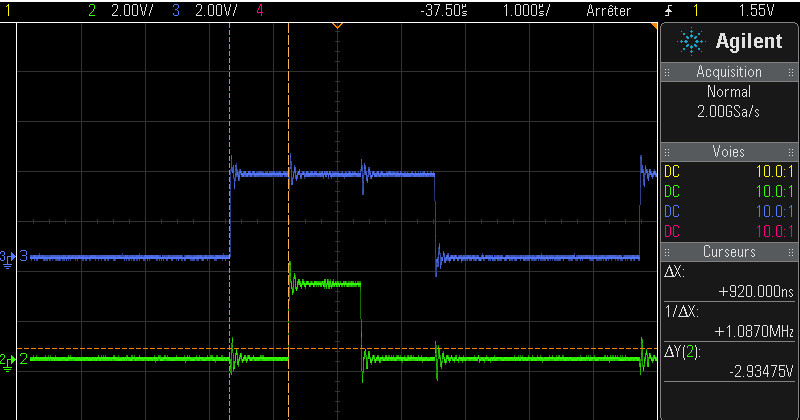
Now we come to the critical question: can EIC_Interrupt_Handler respond to changes on A3..A0 with a new value on R within 500ns?
My research suggests the answer is maybe, but it will be difficult. I found two discussion threads where people were attempting to do something similar with Atmel SAM Cortex M4 and M7 microcontrollers. The first used a 300MHz SAME70, and found a 300ns latency to the start of the interrupt handler. The second used a 120 MHz SAM4E and found a 200ns latency to the start of the handler. These are the delays from the input pin transition to when the interrupt handler begins to run, and they don’t include the actual execution time of the interrupt handler, which is probably several hundred nanoseconds more.
Why so slow? First, the Cortex M4 has a built-in interrupt latency of 12 clock cycles. That’s to do whatever the hardware does for interrupt processing – save the execution state, fetch the interrupt vector, and whatever other voodoo is required. At 120 MHz that’s already 100ns gone.
Then the first instruction of the interrupt handler code must be fetched from internal flash memory. At 120 MHz, the flash isn’t fast enough to supply data in a single clock cycle. It requires 5 wait states, so a read from flash memory needs 6 total clock cycles. That’s another 50ns. So even in the theoretical best-case performance, it will still be a minimum of 150ns before the interrupt handler can begin to run. The two real-world examples I mentioned above were slower.
What about these flash wait states? Does it mean that every instruction in the interrupt handler will need 6 clock cycles to load from flash? I don’t understand the details, but the answer is no. There’s some prefetching and caching happening. Also most instructions are 16 bits wide, and the flash has a 128 bit width, so several instructions can be prefetched and cached at the same time. At least for straight line code with no jumps, I’m guessing that the rest of the interrupt handler can run at speeds approaching 1 instruction per clock cycle at 120 MHz. If anybody knows of good reference data for this, please let me know.
If the flash wait states are a major problem, it may be possible to copy the interrupt handler code to RAM and run it from there. I’m assuming the internal RAM has zero wait states, but I might be wrong on that point.
So 150ns before the interrupt handler can begin to run leaves 350ns remaining. That’s 42 clock cycles at 120MHz. So the interrupt handler can be up to 42 instructions long, on its longest execution path? Not quite, because some common instructions like STR require two clock cycles. Assuming an average time of 1.5 clock cycles per instruction, those 42 clock cycles are only enough for 28 instructions. Can EIC_Interrupt_Handler be implemented in only 28 Thumb assembly instructions? Um… maybe?
Complicating Factors
A few other factors raise the difficulty bar further. If the main code ever disables interrupts, or performs any atomic operations, it will delay running of the EIC_Interrupt_Handler and cut further into that 500ns window. In code that uses lots of interrupts, sometimes it’s impossible to avoid needing critical sections where interrupts are briefly disabled, for example to check some value and then set another value based on the first one. Failure to do this can cause rare but serious bugs, if an interrupt intervenes between reading the first value and setting the second.
Another serious complication is the possibility of multiple back-to-back invocations of EIC_Interrupt_Handler. What happens if one of the A3..A0 inputs changes immediately after execution of the line:
registerNumber = ((PIN_STATE & ADDR_PINS_MASK) >> ADDR_PINS_SHIFT); // get A3..A0
The remaining code will output the value of R for the old A3..A0, then the interrupt handler will finish, then a new interrupt will trigger and the handler will be invoked again to process the new A3..A0 input state. The total latency from the change on A3..A0 to the final correct output value of R will be something like 1.5 times the latency for the normal case. In a system where the timing margins are already very tight, that may be enough to break it entirely.
I don’t see any way around this back-to-back invocation problem. Moving EIC_INTFLAG &= ~ADDR_PINS_MASK to the end of EIC_Interrupt_Handler wouldn’t help anything. It would actually clear the pending interrupt flag from the second change of A3..A0 without ever responding to it, resulting in incorrect behavior.
Conclusions
So can this work – is software interrupt processing viable with these kinds of timing requirements? Is there some optimization trick I can use in the interrupt handler to improve things? Should I even spend the time to attempt it? Maybe there’s some clever way to use the built-in CCL programmable logic that I’ve overlooked, to help accelerate the interrupt handler or even replace it entirely? Or should I just write off this idea as too difficult and too problematic, and continue using a separate programmable logic chip for a mux and glue logic? Decisions…
Read 15 comments and join the conversation15 Comments so far
Leave a reply. For customer support issues, please use the Customer Support link instead of writing comments.
IMHO Most of the High end Cortex devices are not intended for microsecond determinism. I would look at something a bit harder, e.g. TI C2000, Marketed for Real Time applications
http://www.ti.com/microcontrollers/c2000-real-time-control-mcus/overview.html
Interesting project! We tackled something just a little like this in the PiTubeDirect project – see github – where we got a Raspberry Pi to act as a smart peripheral to a 2MHz 6502 machine. One thing we did was to trigger our interrupt handler off the decoded Chip Enable signal, at which point we captured the low address bits, the databus, the read-not-write signal. In other words, not triggering off the low address bits, and not using a clock. There’s a bit of an assumption there that the CE is not going to glitch, but that can be handled in the software.
I don’t think you would know unless you test it. This looks to be the only SAMD51 dev board on the market right now: https://www.mattairtech.com/index.php/development-boards/xeno-mini.html Maybe use a FPGA board to generate the worst case patterns and see if the microcontroller can hold up?
SAMs can not only execute code from flash, they can also execute code from RAM. Older SAMs needed that to re-program the flash (flash was not readable during erase and write). I would guess that RAM needs less wait states, so an interrupt handler placed in RAM should be faster.
When using gcc, use __attribute__((section (\”.ramfunc\”))) or the macro RAMFUNC.
Just make sure that the interrupt does not fire until the startup code has copied the interrupt handler code from flash to RAM (before main() is called).
There’s an open-source drive emulator built around the cheap Gotek hardware – https://github.com/keirf/FlashFloppy
The Gotek hardware is built around an STM32 MCU. Whether it can meet the strict timing requirements, I can’t say though.
Dillon, the SAMD51 pinout is nearly identical to the SAMD21, so you could just cut and patch one or two traces on a SAMD21 board. If you don’t plan to use the SAMD51’s built-in switch mode regulator, then there’s almost no difference at all. Or take an existing SAMD21 breakout board design like https://github.com/sparkfun/SAMD21_Dev_Breakout, and make the small changes needed in the design to create a SAMD51 prototype PCB.
I have two options for you, one bad because obscure, wouldnt go that route:
xmos does hard realtime pretty well. They have a pseudo 4/8/16/32 core chips, effectively running cores at ~60-100MHz each. In reality its up to 32 hardware threads taking turns in accessing memory (to hide latency, internally its 1-2 1GHz cpus), but every core/thread gets 1 clock cycle gpio access. You can bitbang things like USB 1.1 or Ethernet no problem, plus you get serdes hardware. Basically its FPGA for non hardware C talking people, just like Propeller P8X32A, except 5x faster.
Something like $5 XS1-L4A-64-TQ48 could work. 4 cores, 16KB single cycle ram per core, up to 100MHz GPIO. No need for interrupts with one 100MHz core dedicated to 1 cycle bitbanging.
One easy street, imo no brainer:
Dual core ARM micro like $7 200MHz LPC4310, again with one core doing all the bitbanging you avoid this whole non deterministic interrupt latency mess. Bonus points 480Mbit USB 2.0 (unlike SAMD51s 12Mbit) with PHY buildin and 168kB SRAM.
Want more bang for buck? $10 LPC4370 has three 200mhz cores and 12Bit 80MHz ADC :o. Used for example in AirSpy SDR Dongle. Very powerful.
Apparently LPC4300 can do IO at core speed(IO on cpu bus, most ARMs used to relegate IO to secondary slower bus which limited IO speed, STM32F103 maxed at 18MHz etc), 50MHz pin toggling in non unrolled loop: https://www.eevblog.com/forum/microcontrollers/what_s-the-fastest-clock-you-have-generated-on-a-gpio-pin-of-an-arm-dev-board/msg832044/#msg832044
Did I mention LPC-LINK2 dev board is only $20?
Good ideas. I’d been thinking a dual core MCU wouldn’t really help, but forgot to explain why in the blog post. A 120 MHz coprocessor (second core) that was continuously polling could run the body of EIC_Interrupt_Handler in a continuous loop instead of as an interrupt service routine. So it could avoid the 12 clock cycles of interrupt latency (100ns). And it wouldn’t have to worry about disabled interrupt windows or atomic operations elsewhere in the code that might delay interrupt processing. But the rest would be the same as with an interrupt-driven design, including what I called the “back-to-back invocation problem”. At best, I think it would make it possible to claw back 100ns of that 500ns window.
But a coprocessor design would have some extra overhead that a single-core design wouldn’t, in receiving the current states from the main microcontroller, and communicating state changes from the write handler back to the main microcontroller. I’m not sure exactly how that would work, but I expect it would require more than zero code and zero time, and make the polling loop slower than it would be otherwise. So probably the net speedup from a coprocessor design would be at best 20% (100ns), and at worst zero or negative due to inter-mcu communication.
I looked briefly at one dual-core mcu datasheet, and it wasn’t clear to me how the two cores communicate. Do they typically share a region of memory? Some shared registers? Or is it just two completely separate microcontrollers with separate IO pins in a single package?
Generally, all RAM is shared-access – some of the more powerful MCUs have separate smaller caches for each core, but you typically just have to not both try to write to the same memory region at the same time AFAIK
It seems to be possible to meet the 500ns on a AtXmega running at 32 MHz.
Time budget from input to output is 16 cycles.
Detect pin change (1 cycle)
Interrupt response time 6 to 10 cycles:
1-4 cycles to finish the ongoing instruction
2 cycles to push PC to stack
3 cycles to jump to the ISR
This leaves 5 cycles for the actual work:
– Save X address register to register pair using MOVW (1 cycle)
– Load high byte of address pointing to LUT into XH (1 cycle)
– Load input pin status into XL (1 cycle)
– Load data from memory (1 cycle)
– Write to output (1 cycle)
(…) further code + cleanup
Notes:
– Since no ALU operation is used, the processor status register does not need to be saved/restored
– Swapping the register pair XL:XH with Rxx:Rxx+1 (MOVW) can be done in a single cycle (compared to 2 using PUSH).
But Rxx:Rxx+1 must not be used by the compiler (-ffixed-rxx flag of GCC).
– One could also prevent GCC from using the X register, this step would speed up things by 2 cycles.
Make the write operation interrupt driven, and have the main loop poll a0-a4. Even a basic AVR running at 16-20Mhz can manage < 500ns latency response:
in ZL, PORTB ;1 cycle read A0-A4
ld r0, Z ;2 cycle indexed read
out PORTA, r0 ; 1 cycle write
rjmp loop ; 2 cycle jump
At 16Mhz, you'd still have a couple cycles to spare, so you could save PORTA before the loop, then ora r0, portatmp inside the loop to avoid clobbering the porta values.
Thanks for the idea! It’s encouraging that you guys think it’s possible. Once I have some real code written, I’ll post a disassembly for some feedback.
The main loop can’t use polling, unfortunately, because it has other work to do (generating the endless bitstream that represents the signal from the virtual read head as the disk spins).
The challenge is not just to achieve < 500ns reaction time to a signal edge on a pin (which I agree is doable), but to perform a useful amount of work within that time (check which of several pins triggered the interrupt, enable and disable pin output drivers, mux hardware peripherals with GPIO on the same pin, and so on - unfortunately not as easy as a simple table lookup) and output a result. And to do this not just once for an isolated edge, but in an environment where multiple edges may occur within 500ns. Which means the ISR for edge 1 may still be running when edge 2 occurs, delaying the start of handling edge 2.
Check this for an overview on interrupt latencies for different MCUs: https://jaycarlson.net/microcontrollers/
>> it may be possible to copy the interrupt handler code to RAM
Yes, both the vector table (see VTOR) and code can be moved to RAM. The D51 has cache to complicate timing, but it also has “tightly coupled memory” (see TCM)
>> multiple back-to-back invocations of EIC_Interrupt_Handler
The CM4 NVIC actually has some features to REDUCE latency in cases like this. See “Tail chaining” – if an interrupt is pending at the time of “return from interrupt”, the NVIC skips both the restore and the new save of the context and goes directly to the new ISR code.
There’s the Event System, which I don’t know enough about to say whether it would be useful. (I’m guessing that it might improve response “sometimes”, which isn’t good enough.)
I’m inclined to agree with others that a CM4 is a poor choice if you need fast and deterministic interrupt handling.
How about a Cypress PSOC chip? My (poor) understanding is that they have a fair amount of FPGA-like logic within the CPU (like the CLC, only lots more. They seem to vary widely on the degress of specialization of the non-CPU bits, though.
A lot of vendors seem to be putting CM0 cores on the same chip with their “more powerful but less deterministic” cores.
Thank for the tip about tail-chained interrupts – that will help a lot!
Part selection is a balance. I’d previously ruled out the Cypress PSoC, because while its built-in logic looks good on paper, it seems weak in tools, example code, example hardware, and especially in hobbyist community support. This low-latency interrupt thing is just one part of a much larger application, and I prefer a more mainstream choice like SAM or STM32 if possible. If I can’t make the interrupt magic work, I’ll take another look at the PSoC, or maybe just add some external discrete logic.