

Archive for the '3D Graphics Thingy' Category
More on Memory
 I’ve been working hard the past week on a DDR2 memory controller for the Xilinx starter kit, and refining my estimates for 3d Graphics Thingy’s memory bandwidth requirements. There’s been progress, but it feels like things are moving at a snail’s pace.
I wrote earlier about some basic bandwidth estimates, and have revised them somewhat here. Assume pixels and texels are 16 bits (5-6-5 RGB format), z-buffer entries are 24 bits, and the screen resolution is 640×480 @ 60Hz. Let’s also assume a simple case where there’s no alpha blending being performed, and every triangle has one texture applied to it, using point sampling for the texture lookup. For every pixel, every frame, the hardware must:
- Clear the z-buffer, at the start of the frame: 3 bytes
- Clear the frame buffer, at the start of the frame: 2 bytes
- Read the z-buffer, when a new pixel is being drawn: 3 bytes
- Write the z-buffer, if the Z test passes: 3 bytes
- Read the texture data, if the Z test passes: 2 bytes
- Write the frame buffer, if the Z test passes: 2 bytes
- Read the frame buffer, when the display circuit paints the screen: 2 bytes
Assume too that the scene’s depth complexity is 4, meaning the average pixel is covered by 4 triangles, and steps 3-6 will be repeated 4 times. Add everything up, and that’s 47 bytes per pixel, times 640 x 480 is 14.43 MB per frame, times 60 Hz is 866.3 MB/s.
The DDR2 memory on the Xilinx starter kit board has a theoretical maximum bandwidth of 1064 MB/s, so that might just fit. I have serious reservations about my ability to later recreate such a high-speed memory interface on a custom PCB, but ignore that for now. Unfortunately you’ll never get anything close to the theoretical bandwidth in real world usage, unless you’re streaming a huge chunk of data to consecutive memory addreses. Even half the theoretical bandwidth would be doing well. I’ll be conservative and assume I can reach 1/3 of the theoretical bandwidth, which means 355 MB/s. That’s not enough. And I’ll also need some bandwidth for vertex manipulations, since I’ve only considered pixel rasterization, and possibly for CPU operations too. It looks like things will definitely be bandwidth constrained.
Fortunately there are some clever tricks that can be used to save lots of memory bandwidth.
- Z occlusion: When a pixel fails the Z test at step 3, then steps 4-6 can be skipped. With a depth complexity of 4, and assuming randomly-ordered triangles, then on average 1 + 1/2 + 1/3 + 1/4 = 2.08 triangles will pass the Z test and get drawn, not 4. That’s a savings of 14 bytes per pixel, or 258 MB/s!
- Back-face culling: When drawing solid objects, it’s guaranteed that any triangle facing away from the camera will be overdrawn by some other triangle facing towards the camera. These back-face triangles can be ignored completely, skipping steps 3-6 and saving 10 bytes per culled pixel. Assuming half the pixels are part of back-facing triangles, then that’s a savings of 369 MB/s. Of course some of the pixels rejected due to back-face culling would also have been rejected by Z occlusion, so it’s not valid to simply add the savings from the two techniques.
- Z pre-pass: Another technique is to draw the entire scene while skipping steps 5 and 6, so only the Z buffer is updated. Then the scene is drawn again, but step 3 is changed to test for an exactly equal Z value, and step 4 is eliminated. This guarantees that steps 5 and 6 are only performed once per pixel, for the front-most triangle. However, step 3 must now be performed twice as many times, and all the vertex transformation and triangle setup work not accounted for here must be done twice. Whether this results in an appreciable overall savings depends on many factors.
- Skip frame buffer clear: If the rendered scene is indoors and covers the entire screen, then the frame buffer clear in step 2 can be omitted. That’s a savings of 37 MB/s.
- Skip Z-buffer clear: If the rendered scene covers the entire screen, then the Z-buffer clear in step 1 can also be omitted, but sacrificing one bit of Z-buffer accuracy. On even frames, the low half of the Z-buffer range can be used. On odd frames, the high half can be used, along with a reversal in the sense of direction, so larger values are treated as being closer to the camera. This means that every Z value from an even frame is farther away than any Z value from an odd frame, so each frame effectively clears the Z-buffer for the next one. This provides a savings of 55 MB/s.
- Texture compression: Compression formats like DXT1 can provide a 4:1 or better compression ratio for texture data. If the rasterizer can be structured so that an entire texture is read into a cache, and then used for calculations on many adjacent pixels, this can translate directly into a 4:1 bandwidth savings on step 5. Assuming less than perfect gains of 2:1, that translates to a savings of 18 MB/s.
- Texture cache: Neighboring pixels on the screen are likely to access the same texels, when the textures are drawn magnified. A texture that’s tiled many times across the face of a triangle may also result in many reads of the same texel. The expected savings depend on the particular model that’s rendered, but are probably similar to those for texture compression, or about 18 MB/s.
- Tiled Z-Buffer: The Z-buffer can be divided into many 8×8 squares, with a small amount of state data cached for each square: the farthest point (largest Z value) in the square, and a flag indicating if the square has been cleared. That’s 25 bits per square, or 15 KB for a 640×480 Z-buffer. That should fit in the FPGA’s block RAM. Then when considering a pixel before step 3, if the pixel’s Z value is larger than the cached Z-max for that square, the pixel can be rejected without actually doing the Z-buffer read. Furthermore, when the Z-buffer needs to be cleared, the cleared flag for the block can be set without actually clearing the Z-buffer values. Then the next time that Z-buffer square is read, if the cleared flag is set, the hardware can return a square filled with Z-far without actually reading the Z-buffer values. This skips both a Z write and a Z read for the entire square. In order to gain the benefit of the cleared flag, the hardware must operate on entire 8×8 blocks at once before writing the result back to the Z-buffer. The total savings for both these techniques is at least 110 MB/s, and possibly as much as 165 MB/s depending on how much is occluded with the square-level Z test.
- Z-buffer compression: 8×8 blocks of Z-buffer data can be stored compressed in memory, using some kind of differential encoding scheme. Like the previous technique, this would require the hardware to operate on an entire 8×8 block at a time in order to see any benefit. The cost of all Z-buffer reads and writes might be reduced by 2:1 to 4:1, at the cost of additional latency and hardware complexity to handle the compression. This could provide a savings in the range of 350 MB/s.
Unfortunately the savings from all these techniques can’t merely be summed, and the savings I’ve estimated for each one are assuming it’s done by itself, without any of the other techniques. However, when used together, the combination of backface culling plus Z-occlusion should provide at least 400 MB/s in savings, texture compression and caching another 30 MB/s, and Z-buffer tiling another 110 MB/s. That lowers the total bandwidth needs down to 326 MB/s, roughly the same as my conservative estimate of real-world available bandwidth.
Read 3 comments and join the conversationFPGA Pong
Everyone working on a video application using an FPGA seems to start with Pong, so why should I be any different? I put together this Pong demo as an exercise to help get more familiar with Verilog, and gain some experience working with the Xilinx tools and the Spartan 3A FPGA starter kit. It was very slow going at first, but things are slowly beginning to make sense to me now. And hey, I’ve got Pong!!
pong.v – Verilog HDL source pong.ucf – user constaints file, with pin-mappings for the Spartan 3A starter kitSome of the ideas were taken from fpga4fun’s Pong tutorial, and the quadrature decoding logic for the rotary knob was ripped from the tutorial verbatim.
I found that the most difficult part to get working was the collision detection. My brain kept getting tripped up by the difference between writing software where statements are executed sequentially, and HDL statements defining a bunch of operations that all happen at once. I ended up with something like this:
always @(posedge clk) begin
    if (collided)
        direction <= !direction;
    if (direction)
        position <= position + 1;
    else
        position <= position - 1;
end
That looks fine for sequential code, but in hardware it didn’t work. When the ball reached a point where a collision was detected, the hardware would switch the direction and increment the position simultaneously. The position increment used the old direction value, since it was happening in parallel. The result was that the ball would move one step deeper into collision territory. On the next clock, it would move in the new direction, but since it had been two steps into collision territory, one step wasn’t enough to get out, so another collision was detected and it reversed direction yet again. This caused the ball to get stuck in the wall. Confused? Me too.
I ended up solving this by introducing an XOR:
always @(posedge clk) begin
    if (collided)
        direction <= !direction;
    if (direction ^ collided)
        position <= position + 1;
    else
        position <= position - 1;
end
I think there must be some more elegant solution, but I didn’t find it.
I also had trouble handling the initial conditions, setting the ball position and direction to appropriate values at startup. Normally I’d do this with a reset line, but I’m not sure how to do it in an FPGA. The Spartan 3A starter kit doesn’t provide any kind of reset input that I could find in the documentation. And at any rate, it would need to reset the logic of the design, without resetting the FPGA itself, which clears the design entirely until it’s programmed again.
I later discovered from James Newman that “initial” blocks are actually synthesizable, so you can do something like:
initial begin
    position <= 200;
end
That blew my mind, because I must have read 100 different Verilog guides that say initial blocks can’t be synthesized into hardware. And yet, it’s true. I’m very curious how this actually works.
I want to review the Pong design, because it feels way more complicated than it needs to be. I described this to James as Verilog making me lazy. It seems way too easy to write some complicated expression involving a dozen equality comparisons, greater/less than comparisons, and ANDs and ORs, when with a little more thought, the logic could probably be substantially simplified. For instance, I think
wire ball = (xpos >= ballX && xpos <= ballX+7);
could be rewritten as
wire [9:0] delta = xpos - ballX;
wire ball = (delta[9:3] == 0); // or even wire ball = ~(|delta[9:3])
which only requires a 10-bit subtractor and a 7-input NOR, instead of two 10-bit comparators and a 2-input AND. Or maybe:
reg[2:0] ballCount;
always @(posedge clk) begin
    if (xpos == ballX)
       ballCount <= 7;
    else if (ballCount != 0)
        ballCount <= ballCount - 1;
end

wire ball;
assign ball = ballCount != 0;
That’s a 3-bit down counter, and a bunch of XORs and NORs. I’m not sure if that’s better, but you get the idea. Once you start writing complex clauses of nested ifs and lengthy boolean expressions, it’s easy to lose sight of the underlying hardware implementation.
Read 11 comments and join the conversationMemory Bandwidth
I did some preliminary memory bandwidth calculations for 3D Graphics Thingy, based upon the discussion in the comments of the previous post, and the numbers aren’t encouraging. Even for the simplest possible case, I don’t think there will be enough bandwidth to do what I’m imagining, let alone any more complex cases involving more interesting rendering effects.
For every pixel, every frame, this is the minimum that must be done:
- Clear the z-buffer, at the start of the frame
- Clear the frame buffer, at the start of the frame
- Read the z-buffer, when a new pixel is being drawn
- Write the z-buffer, if the Z test passes
- Write the frame buffer, if the Z test passes
- Read the frame buffer, when the display circuit paints the screen
That’s 6 memory operations, per pixel, per frame. Assuming a pixel is 3 bytes (one byte each for red, green, and blue), a z-buffer entry is also 3 bytes, the frame buffer is 640 x 480, and the refresh rate is 60 Hz, then that’s:
6 * 3 * 640 * 480 * 60 = 316MB/sec
If the DRAM datapath is 16 bits wide, as is common, then that’s 158 million memory transactions per second, so the DRAM must run at 158MHz. This is maybe within the realm of possibility, but not by much, I think.
A more realistic estimate would involve steps 3, 4, and 5 happening many times, as fragments of different triangles overlap the same pixel. Performing alpha blending would add an additional “read the frame buffer” step for each pixel. And drawing textured triangles rather than flat-shaded ones would involve one or more additional texture memory reads for each pixel. A more realistic memory bandwidth estimate for a scene with an average depth complexity of 4, with alpha blending and texturing, is probably about 1.4 GB/second, requiring a memory speed of 700MHz. That’s definitely out of reach.
There are certainly some tricks I could use to improve things, starting with using several DRAMs in parallel. Unfortunately each new DRAM requires about 40 FPGA pins to interface with it, and since I need to limit myself to low pin-count FPGAs that can be hand-soldered, realistically I probably can’t do more than two DRAMs in parallel. Using a smaller frame buffer or fewer bits per pixel would also help, but that’s trading away image quality, which I’d like to avoid.
Caching seems like it should play a role here, but I’m not sure exactly how. If there are many shader units operating in parallel, they all must keep their caches in sync somehow, or share a single cache. And even if there’s only one shader unit, so cache coherency isn’t an issue, it’s not obvious to me that a traditional cache would actually speed things up. A pixel shader won’t spend lots of time manipulating the same few bytes of memory over and over, the way a CPU does when executing a small loop. Instead, it traverses the interior of a triangle, visiting each pixel exactly once. The next triangle it processes is unlikely to have any overlap with the previous one. Given these patterns, a cache probably won’t help.
Read 14 comments and join the conversationFPGAngst
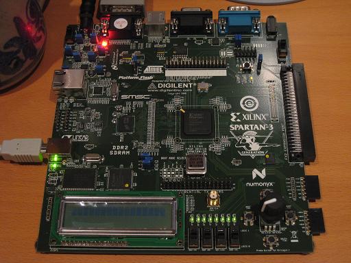
I’ve spent the past few days getting familiar with my Xilinx Spartan 3A Starter Kit, and so far, it’s not going well. I’d thought I was pretty competent with the basics of digital electronics, and the concepts of HDL programming and FPGAs. But working through a “blink the LED” example using the Xilinx ISE WebPack software has been an exercise in frustration. The learning curve is more like a brick wall, and I’m getting dizzy from banging my head into it over and over.
I’ll begin with the starter kit itself. Given the name, you might think it’s aimed at people who want to get started with FPGAs. Forget it. I was very disappointed to find that the starter kit came with almost no documentation at all. Instead, it just had a DVD with a two year old version of the ISE software (now two major releases out of date), and a leaflet with a URL to find more information. The only printed documentation was for the Embedded Devlopment Kit, which is a separate product and doesn’t even work with the free version of the Xilinx ISE. Following the URL, I found the manual for the starter kit, but it’s little more than a catalog of all the hardware on the board. If you want any kind of tutorial for an FPGA “hello world” using this board, or a high-level overview of the various steps involved in creating and programming an FPGA design, or any kind of “starter” information at all, you’ll have to look elsewhere.
Plowing through the ISE software on my own, the first issue I faced was the need to choose what FPGA model I wanted to target. You might think there would be a predefined choice for “Spartan 3A Starter Kit”, but you’d be wrong. After some digging, I found that the starter kit has a XC3S700A, but that wasn’t enough. I needed to specify what package it was, and what speed grade too. How do you tell this? It’s mentioned nowhere in the starter kit manual. After about 20 minutes of searching around, I finally managed to find the web page that deciphered the tiny, near-illegible numbers printed on the chip to determine the package and speed. It’s FG484-4, if you’re keeping score at home.
The ISE itself is really bewildering. It’s basically a shell application that coordinates half a dozen other tools, each of which has its own UI and terminology. The other tools look like old command-line apps that someone slapped together a GUI for using Tcl/Tk. The ISE uses a strange (to me at least) “process” metaphor, which is a context-sensitive subpanel that fills with different actions, depending on what you’ve selected in the main GUI. It took me two days of hunting to figure out what I needed to click on to make the simulation-related process options magically appear. The processes are also arranged in a hierarchical list, so in most cases, running a process requires running all the ones in the tree before it. I still haven’t figured out how to check if my Verilog compiles without doing a complete synthesize, place, and route for the entire design.
Other ISE headaches:
- The GUI-based Plan Ahead tool used to assign signals to physical pins bears no relation to the text-based UCF (user constraints) file examples in the starter kit online manual.
- ISE keeps getting confused about the UCF file, and I have to remove it from the project and re-add it. It’ll complain that I don’t have a UCF file, then when I try to add one, it complains there already is one.
- Integration with iMPACT (the programming tool) is apparently broken. ISE says it’s launching it, but doesn’t. iMPACT must be launched manually.
- After using a wizard to create a DCM module to divide the input clock by two, there’s no “results” page or other info that defines what ports the wizard-created module has. It doesn’t let you actually look at the module code: clicking on it just relaunches the wizard. I had to go poke through random files on disk to discover the module ports.
In comparison to the software, the hardware itself seems pretty good, but maybe a little TOO good. There are no less than four different configuration EEPROMs that can be programmed, with a complicated system of jumpers for controlling which one to program and which to use at startup. This just makes life more complicated than it needs to be.
The only big negative about the hardware is that there’s no SRAM at all. I don’t know how I missed this when I was looking at the specs. Instead, it has 64MB of DDR2 SDRAM. Yeah, that’s a lot of RAM, but creating a memory controller interface for DDR2 RAM is a big honking complicated task all in itself. That means that if you want to do any kind of project involving RAM, you either need to be content with the few kilobytes of block RAM in the FPGA itself, or go on a long painful detour to design a DDR2 memory controller first. The 133MHz oscillator for the DDR2 RAM also occupies the only free clock header, so it’s impossible to introduce another clock to the design (for example, a 25.175MHz oscillator for generating VGA video).
Stumbling blindly through the software, I did finally manage to design, simulate, program, and run a simple example that blinked three LEDs. I’m sure everything will make more sense in time, but it’s hard for me not to feel grumpy right now. I feel like I’m spending all my energy wrestling with the tool software, and none on the project itself. In short, it feels like a software project, not a hardware one. I’ve barely touched the board, other than to plug in the USB cable and flip the power switch. My multimeter, chip puller, wire stripper, and other tools sit unused in my toolbox. Instead, I’m spending time reading a lot of manuals and guessing at what some opaque piece of software is actually doing under the hood. The experience with the clock generation wizard was downright depressing: it just writes some HDL code for you and doesn’t even let you see it, so you’re at least two levels removed from having a prayer of actually understanding what’s going on. Since my end goal in all my homebrew hardware is to gain a better understanding of how things work, that’s especially galling.
I’m going to search out some more ISE tutorials and any other good learning tools I can find, but I’m also going to take another look at the Altera tools. I’ve heard that the Altera software is more beginner-friendly, but I went with Xilinx becuase their starter kit appeared more powerful. I’m now realizing that the quality of the software tools and ease of the development experience is much more important than the number of gates on a particular FPGA. Altera’s Cyclone II starter kit isn’t as full-featured as the Xilinx kit I have now, but it’s decent, and it has some SRAM too. More than likely, the Altera tools will just be a different flavor of incomprehensibility, but it’s worth a look.
Read 37 comments and join the conversationFillRect
OK, time to get back to 3D Graphics Thingy! 3D graphics rendering, implemented in hardware. Here we go. Starting right now. Any time now. 1, 2, 3, go. Getting ready, this is it, here we go. OK, really, going to start now.
I stared at a blank sheet of paper for a long while yesterday, and realized I have no idea what I’m doing. How do you make a digital circuit that draws stuff? Where do you even start?
Assuming I had some video memory, and a circuit to display the contents of video memory, I might implement a FillRect function in C like this:
void FillRect(int left, int top, int right, int bottom, int color) {
    for (int y=top; y<=bottom; y++) {
        for (int x=left; x<=right; x++) {
            memory[x][y] = color;
        }
    }
}
Taking this a little further, I could assume a screen width and height of 256 pixels, and one byte per pixel, for a total video memory size of 64K. That would enable me to directly use the X and Y coordinates of a pixel to determine its memory address, by using Y as the upper 8 bits of address, and X as the lower 8 bits. The revised C code would be:
void FillRect(uchar left, uchar top, uchar right, uchar bottom, uchar color) {
    for (uchar y=top; y<=bottom; y++) {
        for (uchar x=left; x<=right; x++) {
            memory[(y<<8)|x] = color;
        }
    }
}
Now how do you build hardware to do that? After more staring at a blank sheet of paper for a while, I started drawing things, and eventually came up with this:

My scrawl is difficult to follow, so I cleaned it up in a drawing program. In the diagram below, the data path is drawn in blue, and the control path in orange. All the control signals are assumed to use positive logic for clarity (1 = active), although in a real circuit with real chips, most would actually use negative logic. The five blue boxes along the top are all 8-bit registers, something like a 74HC377. The two darker blue boxes for X and Y are 8-bit counters, like a 74HC393 maybe. For the counters, I assume that their load input takes priority over their count input, if both are asserted simultaneously. The two boxes labeled “=” are comparators that output true when their inputs are equal, like a 74HC688. The orange run box is a single flip-flop with synchronous set and reset inputs.

How does this work? Initially run is false, so the output of the AND gate connected to the RAM’s write input is also always false, and nothing gets written. To start things going, the CPU (not shown) writes the desired values to the bottom, top, left, right, and color registers for the rectangle to be filled, and then asserts start. At the next clock edge, three things happen:
- run is set to true
- Y is loaded from top
- X is loaded from left
Notice the clock signal itself is used as a control signal, connected through an inverter to the AND gate feeding the RAM’s write input. On the next clock cycle following start, during the second half when the clock signal is low, the output of the AND gate becomes true, and the value in the color register is written to the address specified by the X and Y registers. Oh my God, a pixel was just filled!
The X register’s count input is connected directly to true. At the next clock edge, X is incremented by one, and on the next clock cycle, the neighboring pixel one spot to the right is filled. This continues until X reaches the value stored in the right register, at which point the output of the comparator becomes true. This forces X to be reloaded with the value from left (load preempts count), and also increments Y by one, accomplishing a movement to the start of the next line.
Eventually the filling operation reaches the last pixel of the last line, when Y equals bottom and X equals right, and the output of both comparators becomes true. This resets the flip-flop, forcing run to false, and disabling any further writes to video memory. The FillRect operation is complete.
With work, this FillRect hardware could be generalized to FillTriangle hardware more similar to what 3DGT will need. If left and right were initially equal, and then incremented or decremented by a fixed step on each new line, then flat-bottomed triangles of any shape could be drawn. The per-line steps for left and right would be the inverse slopes of the triangle edges. To draw any general triangle without the flat-bottom limitation, the same circuit could be used again in reverse to draw a flat-top triangle connected to the first flat-bottom one. Alternatively, the hardware could be extended to draw the complete triangle directly, by adding a new knee register, and changing one of the line slopes when Y reaches knee.
Read 3 comments and join the conversationFPGA Research
Over the past few days I’ve done a huge amount of reading about both 3D graphics hardware and FPGAs, and I’m starting to get a better picture in my mind of how this 3D Graphics Thingy might be built. My surprising conclusion is that 3DGT may not require any custom hardware at all, but could be entirely implemented using an off-the-shelf FPGA development board. This is either good or bad, depending on your point of view.
Looking back at my earlier “construction notes” posting, I described a vision of 3DGT as a single-board computer with a CPU, FPGA, RAM, ROM, keyboard, USB, and VGA output. That more or less exactly describes an FPGA development board. All the work would then go into creating the HDL for the graphics pipeline, which would be programmed into the FPGA, turning 3DGT into a mostly firmware project. There would still be a few missing hardware pieces when using an FPGA development board, however:
- CPU – I still need a CPU to drive the graphics pipeline, and determine what to draw. Some high-end FPGAs actually have a CPU built-in, but those are out of my price range. My first approach will be to embed a “soft CPU” into the FPGA along with everything else. Xilinx provides a PicoBlaze 8-bit soft CPU that only consumes about 5% of the space in a Spartan 3 FPGA. There’s also the OpenRISC soft CPU from OpenCores.org, if something more powerful is needed. And if a soft CPU doesn’t work out, I can add a real CPU on a daughter card, attached to the development board’s expansion connector.
- VGA – There are lots of development boards with integrated VGA hardware. However, the cheaper boards are all limited to a few bits per color channel. The best I’ve seen is 4:4:4 12-bit color. That will be great for initial testing, but ultimately I’ll need to add a separate 8:8:8 video DAC on a daughter card.
- Joystick, etc – Connecting a gamepad will require a bit of custom hardware, also on a daughter card. Any sound hardware would need to be external to the daughter board too. For initial testing, I can use the built-in keyboard connection.
I like where this is going, although it’s a lot less hardware-oriented than I’d initially expected. Essentially, I can purchase an FPGA development board and get started immediately, using a soft CPU, low bit-depth VGA, and keyboard input. Once the guts of the graphics pipeline are mostly working, I can expand by adding a daughter card with a CPU, video DAC, gamepad connector, etc. For the final version I might create a custom single-board PCB for exactly the hardware I need, and ditch the development board, or just keep the development board + daughter board as the final hardware.
The development boards I’m considering are Xilinx’s Spartan-3E Starter Kit and Spartan-3A Starter Kit. These seem to be the best fit as far as including the parts I need, without a lot of other parts I don’t need, or costing a million dollars. There’s also a wealth of information and tutorials online about how to use these boards, from Xilinx and third parties.
Both boards include the FPGA, 32MB RAM, 16 or 32MB Flash ROM, VGA, USB, PS/2 keyboard input, two serial ports, ethernet, and a two-line LCD. I don’t need the serial ports or Ethernet, of course, but there they are. Both kits come with 50MHz clock oscillators built-in, but I couldn’t find any data on their maximum possible speeds, or the speed grades of the specific FPGAs.
- 3E – The $149 3E is the older board, with a XC3S500E sporting 10476 logic cells, 360K bits of block RAM, and 20 dedicated multipliers. The major drawback is that the VGA output is 1:1:1, allowing for just 8 colors. That would let me work on triangle rasterization, but not color interpolation or texturing. If I ever want to ditch the development board and make a custom PCB, though, the 3E kit is the way to go. The exact same FPGA is available from Sparkfun in a breakout board, as well as from other vendors, or it can also be purchased as a bare IC with leads that I can solder myself.
- 3A – The $189 3A is the newer board, hosting a XC3S700A. The 3A has 13248 logic cells, 360K bits of block RAM, and 20 dedicated multipliers. The larger number of logic cells is nice, but the big advantage of this kit is the 4:4:4 VGA interface, enabling 4096 colors. The drawback is that if I later want to drop the development board and make a custom PCB, it’ll be difficult to do without switching away from the 3A. It’s only available in a leadless BGA package that I can’t hand-solder, and I haven’t found any 3A breakout boards or adapters advertised online.
Along with all this research into the development hardware, I also did some reading about other similar 3D graphics FPGA projects, hoping I might learn from them. Maybe I didn’t dig hard enough, but I didn’t find much, and what I did find were all unfinished projects:
- Manticore – A project started by two students at the University of Alberta in 2002, but never finished. They implemented a basic rasterizer that will be very interesting to examine, as well as a memory controller to arbitrate memory requests and talk to DRAM. They never worked out all the bugs in the rasterizer though, and the design lacks a z-buffer and texture mapping.
- Niklas Knutsson Thesis Project – A 2005 Master’s thesis from Linköping University, Sweden. This is a great description of the task of implementing a 3D graphics pipeline in an FPGA, but the implementation was never finished. He got as far as drawing some basic test patterns, but most of the design time was spent on the CPU and memory controller, so the 3D pipeline wasn’t fully fleshed out. The HDL source and schematics don’t seem to be available online, unfortunately.
- Open Graphics Project – This is an ongoing project to build a fully PC-compatible graphics card, using a pair of FPGAs on a PCI card. Coincidentally, it was featured on the front page of Slashdot just yesterday. The majority of the development so far appears to have centered on the PCI interface, and support for legacy VGA modes. The documentation on the 3D pipeline is fairly skeletal, and it appears that little of it has actually been implemented so far.
I’m surprised there aren’t more projects out there like this, and apparently none that were ever successful. I’m guessing that such projects do exist, and I’ll just have to dig a little deeper to find them.
Read 7 comments and join the conversation