

Board Layout
While updating the BMOW documentation, I came across this diagram of the main system board layout that might be interesting to share. It shows every part on the board, and howthey’re all grouped into the subsystems that form the computer. Related parts are adjacent most of the time, but I did make some blunders.
Compare the diagram with the photo, and click either one to see a higher-resolution version. They match exactly, except for RAM1 (lower-right of the diagram), which I never got around to placing on the main board.
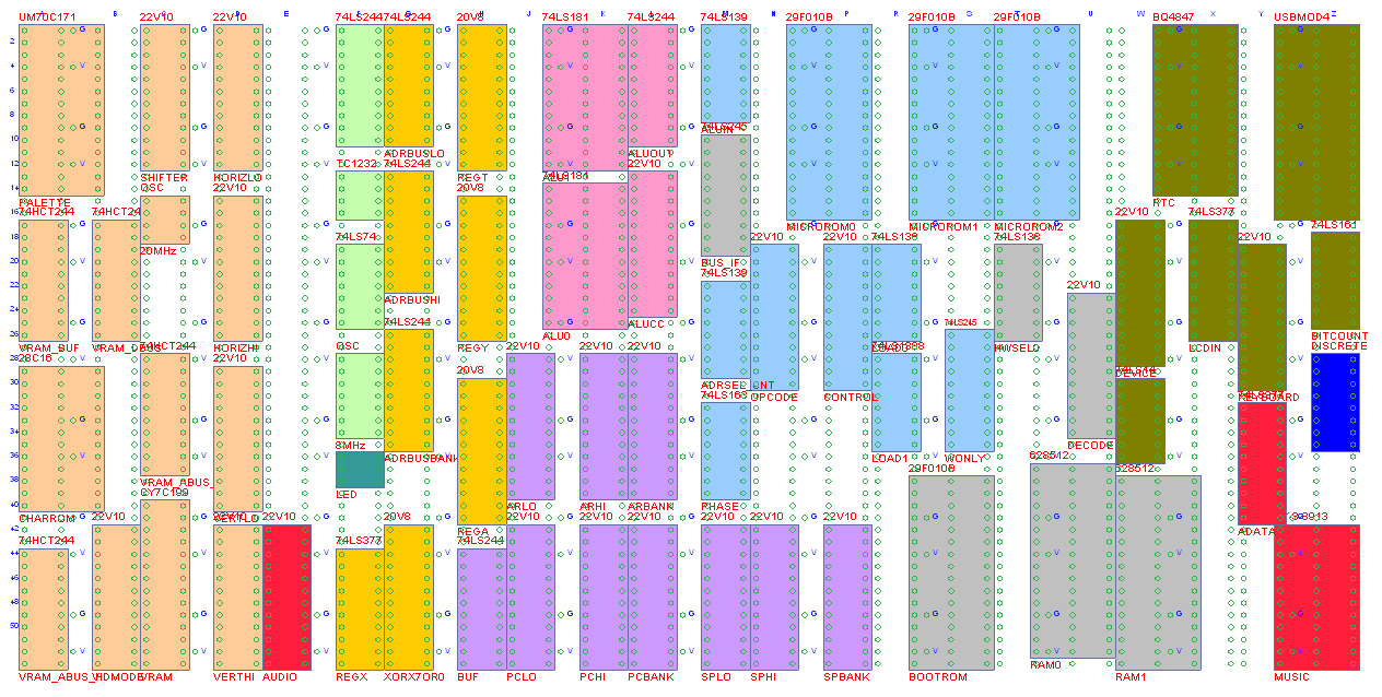

The core systems which form BMOW’s custom CPU are in the center of the board, shown in light blue, pink, orange, and purple. The rest of the systems are arrayed around the outside.
- Control (light blue): Here’s where the control signals are generated to enable and coordinate everything else. It includes the three microcode ROMs, opcode register, instruction phase counter, and related demultiplexers.
- ALU (pink): The mathematical and logical functions are all performed here. It’s a bit of glue circuitry along with a pair of 74LS181s.
- Address Registers (purple): The program counter, stack pointer, and scratch address register are all 24 bits wide.
- Data Registers (orange): There are three user-visible 8-bit registers named A, X, and Y. A fourth register named T is used internally by the microcode.
- System Clock (light green): An 8MHz oscillator is used along with some flip-flops to generate two 2MHz clocks, one 90 degrees out of phase with the other. The power-on reset circuit is also part of this subsystem.
- Memory (gray): The system has 512K ROM, 512K RAM, and the address decoder. I originally planned for two RAM chips and a total of 1MB of RAM, but later decided that was overkill.
- Devices (dark olive): External hardware is mapped into the CPU’s address space. There’s a real time clock, and interfaces for USB, the keyboard, and the LCD front panel.
- Discrete (dark blue): I lumped together all the miscellaneous resistors and capacitors that were needed into a single component carrier.
- Video (tan): Four GALs serve as row and column counters to generate sequential video memory addresses during the display of each video frame. There’s 32K of VRAM, and a separate 2K character generator ROM. A palette chip pulled from an ancient video card translates VRAM values for each pixel into analog R, G, and B voltages for the monitor. There’s also some demultiplexing circuitry to let the VRAM address bus be driven by the row/column counters or by the CPU address bus. The video system has its own clock, which runs at 25.175MHz.
- Audio (red): Some support chips and an AY-3-8913 programmable sound generator create three voices of modified square wave goodness. The three analog voltages for the voices are generated on-board, but the stereo mixing and amplification are done on a small daughter board.
1 Comment so far
Leave a reply. For customer support issues, please use the Customer Support link instead of writing comments.
Это здорово. Такому терпению и трудолюбию можно только позавидовать.