

Archive for the 'Tiny CPU' Category
Tiny CPU Update
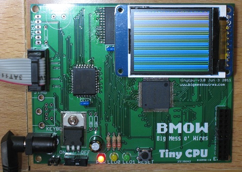
Slow progress continues on the assembly and first boot-up of Tiny CPU. The photo shows a sample program written in Tiny CPU assembly language, drawing a color pattern on the LCD. The serial port and keyboard interface haven’t yet been added to the board, but the Max II CPLD, SRAM, and Flash ROM are all working fine from both an electrical and a design standpoint. After the initial round of swearing at the soldering iron, there were no further electrical problems at all, so all the work has been on configuration and software. The goal of designing a novel CPU architecture and implementing it in hardware has been met successfully.
Of course it’s not all roses and sunshine, and several smaller problems plus one big one have slowed progress and cast doubt on future direction. Debugging has been a major challenge. When things don’t work as expected, or do nothing at all, there aren’t many good tools to help diagnose the problem. The best tool I’ve found thus far is TopJTAG Probe, a $100 software program that lets you examine the current state of any pin, and display continuously-updating state data in a waveform-style window. It’s great for examining external signals at the pins, but the internal machine state remains invisible. It’s also limited to about 400 samples per second due to its use of JTAG boundary scan, which requires slowing the CPU clock to around 100 Hz to do any debugging. My free trial expires in 17 more days, and I’m undecided whether I’ll purchase it.
Altera also offers system debugging tools, including a scriptable Tcl console, in-system sources and probes, and a virtual JTAG interface. Not surprisingly, these tools all require on-chip logic resources, and Tiny CPU has few LE’s to spare. The most promising tool looks like their Signal Tap II logic analyzer, but it requires on-chip RAM, and the Max II has none. Altera doesn’t appear to offer any tools that work purely through JTAG boundary scan without any on-chip logic resources, like TopJTAG Probe. I thought the jtag_debug interface of the scriptable Tcl console might be what I was looking for, but I was unable to get it to work.
When the CPU is running, it’s pretty slow. It took four seconds to fill the LCD with the color test pattern shown in the photo. Much of that is due to the inefficiency of the bit-banged SPI code I wrote to communicate with the LCD, but the 2.6 MHz clock speed is also a factor. The 2.6 MHz is provided by the Max II’s on-chip oscillator, whose frequency is fixed. It can be divided down using logic if a slower clock is needed, but it’s not possible to go faster than 2.6 MHz. According to the timing analysis report, the CPU should run at up to 40 MHz.
Design Disaster
The biggest problem by far is the bank-switching design. Tiny CPU has a 10-bit address space, enabling 1K to be addressed directly. The companion module Tiny Device performs bank switching, mapping 128 possible 512-byte banks of RAM and ROM into the lower and upper halves of the CPU’s address space. When I first described Tiny CPU’s bank switching design, it seemed a clever and elegant way to expand the address space. After working with it in real programs, however, it feels like a complete disaster. It’s confusing and cumbersome. It complicates the design of the programs, the assembler, and Tiny Device. It makes simple things hard. In short, it needs to be taken out back and shot.
Jumping between routines in different banks requires locating the code such that the first instruction of the routine in the target bank is at the next consecutive address, modulo 512, after the instruction in the source bank that alters the bank register. In this way, execution “falls through” to the target bank, transparently to the CPU, by altering the bank register. In practice I’ve found it very difficult to line up the addresses of entry and exit points in different banks. There’s probably some way to abstract it into a general jump table in each bank, but I haven’t found it yet. Adding a new “far call” CPU instruction might help, but I’m very reluctant to embed knowledge of the bank register in the CPU itself, since at the moment it’s just a memory-mapped port handled by Tiny Device.
Given time, the bank-swapping procedure may seem more intuitive and less onerous, but I’m skeptical. And unfortunately 1K is small enough that programs need to deal with bank swapping a lot. It’s even more common than it seems at first, since the upper half of the CPU address space is always mapped to a fixed block of RAM, so programs running from ROM really only have 512 bytes of space to work with before they need to worry about swapping.
Ideally I’d like to increase the address space to something larger, but that would force major changes all over. The 16-bit instruction encoding uses 6 bits for opcode and 10 bits for address, so a larger address space would mean larger instructions. The assembler would need to be substantially altered. And of course the Verilog source for Tiny CPU and Tiny Device would need major alterations as well. My enthusiasm for such a large refactoring right now is pretty low.
Maybe the best use of Tiny CPU is as a small soft-core to incorporate into larger FPGA designs, where a simple microprocessor is needed and the 1K address space limit is not a problem. It would offer an even smaller alternative to soft-cores like PicoBlaze, and be easily portable to any vendor’s FPGA hardware. In this scenario, Tiny CPU would be used alone without Tiny Device, and the RAM and ROM would likely be FPGA logic resources rather than actual external components.
I leave tomorrow for a 10-day trip, so I’ll think it over while I’m away and decide how to proceed with Tiny CPU development when I return.
Read 3 comments and join the conversationJTAG, EXTEST, and hair loss
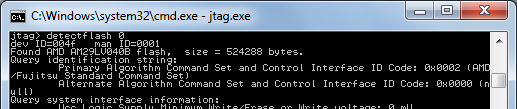 Oof. See that window to the left? That’s the result of 10 hours of debugging effort on bring-up for my custom Tiny CPU board. What you see is UrJTAG connected to the JTAG interface of the Max II CPLD, and successfully detecting the 29LV040B flash ROM that’s also on the board. Getting to this point was a long process covering everything from software to cleaning up bad solder joints.
The good news: I’ve soldered the Max II CPLD, Flash ROM, and SRAM to the board, and they seem to be working. By using UrJTAG and the EXTEST instruction, it’s possible to disconnect the CPLD’s core logic from the pins, and set the pin states to any arbitrary values. The software also needs to be told which pins are connected to the address bus, data bus, CS, OE, and WE. Once that’s done, it’s possible to read and write any non-JTAG device whose pins are connected to the CPLD, by bit-twiddling the CPLD pins. Using UrJTAG’s commands for memory access, I’ve successfully written and read from the on-board SRAM, and reprogrammed the on-board Flash ROM. That should be nearly everything that’s needed to start work on the Tiny CPU core itself.
Interaction with the Programmed Design
I find JTAG and especially the UrJTAG tool to be maddeningly difficult to understand. Things don’t work how I’d expect, or don’t work at all, and I can’t be certain if it’s a hardware problem, software bug, or misunderstanding on my part. The best example is the reason that it took me so long to reach the point where the Flash ROM was successfully detected: interaction between the core logic (the design programmed into the CPLD) and the EXTEST pin manipulation. From what I’ve read, there should be no interaction. When the EXTEST instruction is executed by the JTAG controller, then the pins should be decoupled from the core logic. It shouldn’t matter at all what design is programmed into the CPLD, what that design wants to do with the pins, or whether any design is programmed at all.
After long experimentation and electrical testing, I discovered that the core logic design does matter when interfacing to other devices with EXTEST. Whether this is normal, or the result of a boundary scan software bug in UrJTAG, I don’t know. What I found is that if I programmed the CPLD with a design that declared the data bus as type inout (which it is, of course), then I could read from the SRAM and Flash but not write to them. By sticking a multimeter on the pins, I found that data bus pins driven to a logical 0 using EXTEST worked fine, but data bus pins driven to a logical 1 just went into a high-Z state instead, so I could never write a ‘1’ bit. I also learned that if I set the data bus type as output, then I could no longer read from the RAM or Flash. Only when I set the data bus type to input could I both read and write using EXTEST. This is nonsense on a several levels, as it shouldn’t be necessary to reprogram the CPLD with a new design just to use the EXTEST functionality. The only explanation I can think of is that the boundary scan register uses 3 bits to define the state of each pin (input, input with pull-up, output driving 0, output driving 1, output driving Z, and a few others) which UrJTAG may not handle properly, with some bits carrying over from the programmed design. I had a similar problem when using a trial version of TopJTAG Flash Programmer, however, so I’m not sure I can blame the software.
JTAG Bit-Banging
As another example of UrJTAG strangeness, the board has an LED connected to IO97, such that the LED illuminates when the pin value is 0. It should be possible to blink the LED using UrJTAG’s set signal command, e.g:
jtag> set signal IO97 out 0
After much tearing out of my hair, I learned that while that’s part of it, it’s also necessary to explicitly put the device in EXTEST instruction mode first, and explicitly shift the instruction and data into the device, as UrJTAG does none of this for you:
jtag> instruction EXTEST
jtag> shift ir
jtag> set signal IO97 out 0
jtag> shift dr   (the LED turns on)
A little cumbersome, but at least it works. In contrast, I was never able to get the corresponding get signal command to work at all. After setting IO97 to 0 as above, which visibly turns on the LED, the value of IO97 still reads as 1:
jtag> get signal IO97
IO97 = 1
jtag> shift dr
jtag> get signal IO97
IO97 = 1
The ability to twiddle pins arbitrarily through JTAG could be a huge aid to debugging, but not if the corresponding ability to read the current pin state doesn’t work.
If anyone has some experience using UrJTAG for this kind of troubleshooting, please leave a comment, or contact me by email. Thanks!
Read 5 comments and join the conversationSoldering, with Profanity
Hot diggety damn! I believe I’ve successfully soldered the Max II in its cruel 100-pin package with 0.5 mm pin spacing. At least, I’ve assembled enough of the board to connect it to a JTAG programmer, program an LED blinky routine to the Max II, and confirm that it works. There could still be all kinds of pins shorted or broken, of course, but at least I know I didn’t fry it completely.
Soldering that chip wasn’t fun. It took me about two hours just for that single TQFP 100. I used the drag soldering technique, where you goob tons of solder onto the pins and create pin-to-pin solder jumpers like crazy, then go back afterwards with solder wick to clean up the jumpers. At least that’s the idea.
I had the absolute worst time trying to wick away the jumpers. No matter what I did, the extra solder on the pins wouldn’t soak into the solder wick. I set the wick on top of the pins that had jumpers, then set my iron on the wick, and pressed down onto the sandwich. The solder underneath the wick would melt, but it wouldn’t go anywhere. When I removed the iron and wick, the jumpers remained right where they’d been, with nothing at all soaked into the wick. I applied flux everywhere, over and over, but it didn’t help.
This pattern went on for ages, and I got more and more upset. I started swearing at the board, using every profanity I could think of. I had to close the windows so the neighbors wouldn’t hear. After a while, I started singing random profanities to the tune of opera while I worked on the jumpers. I burned the soldermask off several of the traces, burned the board, and re-heated the same pins so many times that I was certain nothing was left inside the chip but melted slag. All in all, it was not a good time.
Eventually I stumbled onto a few techniques that helped a little, raising my wicking success rate from 0.1% to maybe 20%.
- Some jumpers can be cleared simply by touching the iron briefly to the pins, without any wick.
- Don’t stretch out the wick braid. Keep the strands pressed together, like stranded wire.
- If a stubborn bit of solder refuses to be wicked away, add more solder. A huge glob is actually easier to remove than a tiny fleck.
Assuming the other as-yet-untested pins on the Max II are OK, then assembling the rest of the board should be cake.
Read 4 comments and join the conversationTiny CPU Boards
 The Tiny CPU boards arrived yesterday from Seeed Studio’s Fusion PCB service. Now it’s time to break out my soldering iron again, and get busy with that 0.5 mm pitch 100-pin TQFP. Ugh!
I placed the order with Seeed on June 6, and received the boards on June 23, so that’s 17 days of calendar time from order to mailbox. Considering how slow shipping from China can be, I’m pretty happy with that. It’s actually not much slower than the 12 day turn-around time I got from Dorkbot PDX’s PCB service, which is done in the USA.
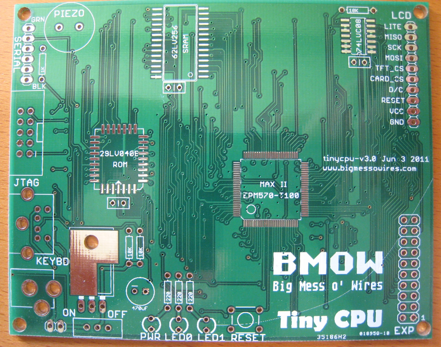
The Tiny CPU board is 100mm x 80mm, or about 12.4 square inches. For 10 boards with 50% e-test, the cost was $25 plus about $7 for shipping. I actually received 12 boards instead of the promised 10. Five boards were taped together and marked with a black line down the edge, so I assume those are the ones that were e-tested. The other seven boards were stacked on top, then the whole bundle of 12 boards was shrink-wrapped, packed in bubble wrap, and packed in a small box for shipping.
The quality of the boards looks pretty good, especially considering the dirt cheap price. Drill holes look nicely centered, and tracks look neat and clean. It’s not all perfect though, and the overall quality level feels a bit less than the Dorkbot PDX boards. There’s a bit of variation in soldermask and plating from board to board, and some of the boards look pretty scuffed up. There are also some odd numbers and a line that were added to my silkscreen layer, which I could do without.
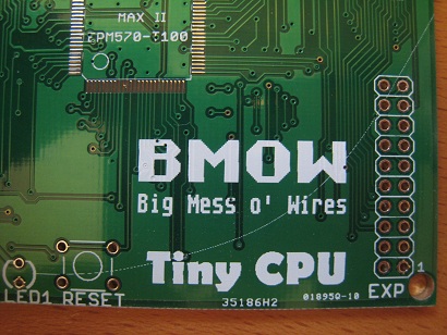 Um, what the heck is 35186H2 and 01895Q-10? And moreover, what is that curved arc in the silkscreen layer extending from LED1 all the way to the board’s edge? None of that appears in my top silkscreen Gerber. It’s not a huge deal to have some random extra numbers and lines, it doesn’t affect anything of course, but it’s a bit annoying.
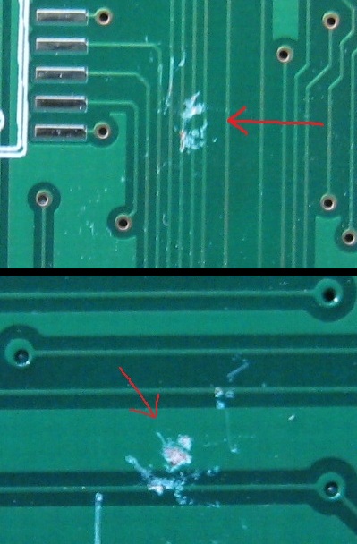 Two of the boards have some pretty significant damage from scraping or impact. I’m not sure if it’s enough to cause a failure, but it definitely might. One board is damaged on the top, and the other on the bottom, and when you stack them the damaged spots overlap. I’m guessing some sharp object got caught between these two boards, and ground away the soldermask where it rubbed against them. Maybe this is why I got 12 boards instead of 10?
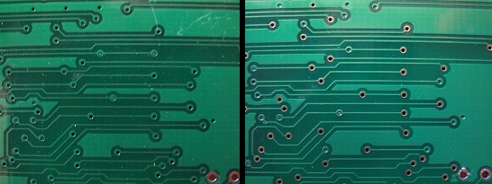 I tented my vias with soldermask this time, or tried to anyway. In theory, 100% of the vias should be tented. In practice, most of the vias are tented, but some aren’t, and the fraction of tented vias varies quite a bit from board to board. Here’s the same section from two different boards, where one is 100% tented and the other is maybe 25%.
Overall I’m fairly happy with these Seeed PCB Fusion boards: decent build quality and cheap pricing. Yes, there are a few dinged and damaged boards, but given the total number of boards for the price (and the two bonus boards I received), I can call those throw-aways and still have a good deal. I would certainly use them again. For smaller boards where the costs are comparable, though, I would favor Dorkbot PDX’s PCB service, since it’s a few days faster and seems to be a bit higher quality.
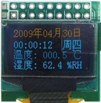
Low-Power LCD Smackdown
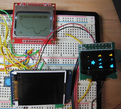 Sometimes it seems like there are a million different LCDs you might use with your microcontroller project, and deciding on one can be hard. Once you’re ready to move beyond a basic text display, you’ll find graphic displays have a dizzying number of options for technology, color depth, interface type, driver, and power. Recently I’ve been collecting info on display options for my own projects, and here I’m presenting three options that look promising.
The Nokia 5110 is a low-resolution monochrome LCD that’s cheap and extremely low-power. A family of small monochrome OLEDs provide crisp, bright displays with a bit more resolution, in a teeny-tiny package. A 1.8 inch color TFT provides even greater resolution and 18-bit color, while still limiting power to about 90 milliwatts.
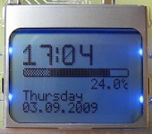 Nokia 5110
Colors: monochrome
Resolution: 84 x 48
Active display area: 2.8 x 2 cm
Interface: SPI
Power: 3.3v
Current: 0.4 mA for logic, 1-10 mA for backlight
Cost: $10
Vendors: Sparkfun, Adafruit
This is the display I’m currently using for my Backcountry Logger project. It’s cheap, easy to use, and consumes very little power. You don’t really need the backlight for daytime visibility, and with backlight off, it consumes just 400 uA! Awesome for battery-powered projects. Just 1-2 mA worth of backlight current is plenty for night-time visibility too, although more would be nicer. This puts the display well within the capabilities of a single CR2032 coin cell.
Working with the display is simple, as long as you remeber it’s a 3.3v device and not 5v tolerant. There are lots of great tutorials and examples available for this display, including this nice one from Adafruit. Communication with the display controller uses SPI. Writing a single byte sets 8 pixels at a time, so pixels are not individually addressable. If you’re mostly displaying text or bitmaps this isn’t a problem, but if you need a more complex image consisting of many overlapping elements, you’ll need to composite them in software before sending the result to the display.
The weak points of the Nokia 5110 display are resolution and looks. The contrast and sharpness are pretty good for a display of this type, but there’s still no getting around the fact that this is a low-res, dark-gray on light-gray display. The 84 x 48 resolution allows for just 14 x 6 characters using a typical 5 x 7 font (allowing for space between letters). If you seek utility, low cost, and low power, it’s a great solution. If you want something with a bit more bling, look elsewhere.
 SSD1306/SSD1308 OLED
Colors: monochrome
Resolution: 128 x 64
Active display area: 2.4 x 1.2 cm
Interface: SPI, I2C, or parallel
Power: 3.3v, and maybe 7-12v
Current: roughly 5-13 mA, depending on how many pixels are lit
Cost: $15-$20
Vendors: Sparkfun (bare LCD), Adafruit, eBay
This little OLED display comes in a few slightly different flavors, but all of them are tiny. It’s one thing to read the dimensions (0.96 inches horizontally), but another to see it in person. All three of the displays discussed here are small, but this particular OLED is smaller than a postage stamp. It’s about the size of the last joint on my thumb.
Despite its small size, the OLED display is very readable. It’s sharp and bright, and a pleasure to look at. Since it’s an OLED, there’s no backlight, and current draw varies between about 5 to 13 mA in my testing, depending on how many pixels are illuminated. The 128 x 64 resolution is a nice bump from the Nokia 5110 display, allowing for 21 x 8 characters. Communication choices are SPI, I2C, or parallel, selectable via configuration pins. Like the Nokia, each byte sets 8 pixels at a time. Adafruit has a tutorial and library.
The display controller chip runs at 3.3v, and the display itself needs 7-12v, although you might be able to get away with a single supply depending on which display variant you have.
Adafruit sells this display on a break-out board, with white pixels, with a SSD1306 controller. The SSD1306 has a built-in charge pump, and can optionally generate 7.5v for the display from a 3.3v supply, which is a very convenient option. Sparkfun sells the naked LCD, with white or blue pixels, and a SSD1308 controller that lacks the charge pump. You’ll need to mount the 0.5 mm pitch connector somehow, and provide a separate power supply for the logic and display. The most common eBay variant comes on a break-out board, with the SSD1306 controller, and yellow pixels in the top quarter and blue pixels in the bottom three quarters. Mine also came hard-wired to use the parallel interface, and switching to SPI required wicking away some solder jumpers and adding new ones.
This display meets a narrower range of needs, but is awesome for its target niche. I’m strongly considering doing a version 2.0 of the Backcountry Logger using this display, to gain the benefit of smaller size, higher resolution, and better looks. Unfortunately with the amount of current it needs, it’s probably outside of what a CR2032 can provide, and will require 2 x AAA or 1 x AAA with a DC boost converter.
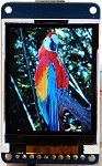 Adafruit 1.8 inch TFT
Colors: 18-bit (262144 colors)
Resolution: 160 x 120
Active display area: 3.6 x 2.8 cm
Interface: SPI
Power: 5v or 3.3v
Current: 1 mA for logic, about 26 mA for backlight (can be dimmed)
Cost: $25
Vendors: Adafruit
This is the display I plan to use for Tiny CPU. Unlike the others, it’s a full color display with individually addressable pixels. It supports 18-bit color, but can also be configured for 16-bit color or monochrome (I think? Haven’t tried that yet). It’s a bit larger than the other two, but still quite small compared to most displays. It is natively a 3.3v device, but the Adafruit breakout board includes an LDO regulator and level-shifter chip, so it can be used with 5v microcontrollers as well. Current demands are the highest of the three displays, but not excessive at about 1 mA for logic and 26 mA for the backlight. The backlight can be dimmed using PWM to further reduce the current. This is still well within the capabilities of an AAA-based battery-powered project.
The TFT is very attractive, not quite on par with the OLED, but certainly nicer than the CSTN used in some other cheap color LCDs. The 160 x 120 resolution feels giant in comparison with the previous displays, allowing for 26 x 15 characters. The display controller allows for a few different protocols, but the break-out board hard-wires it for SPI.
With the larger resolution and greater bit depth, a screen’s worth of data requires many more bytes than the previous two displays. Depending on the speed of your microcontroller and SPI interface, this may result in noticeably slower refresh times. I tested it using hardware SPI on a 16 MHz Arduino, and found the refresh time to be acceptable.
Adafruit has a nice tutorial and library for working with this display (I’m sensing a theme here). Unexpectedly, the breakout board also has a micro-SD card reader on it. Ignore it, or use it as a bonus peripheral in your next project.
Read 6 comments and join the conversationOff To The Board House
 The Tiny CPU board design is now off to the board house for manufacturing. The three week wait begins. Somewhere during that time, the Backcountry Logger boards should come back too.
I selected Seeed Studio’s Fusion PCB service, because it was by far the cheapest prototype-oriented board house for a board this size (12.4 sqin) with multiple copies. I’m a little worried, though, because the Fusion PCB CAM file for Eagle appears to have a bug. I don’t know much about what the CAM file does, other than that Eagle uses it to generate the individual Gerber files from the Eagle .brd file, and all the board houses I’m aware of provide a CAM file you’re supposed to use. Using the Fusion PCB CAM file, and viewing the resulting Gerbers in gerbv, all the drill holes were offset about 250 mils below-left relative to the other layers. You can see this in the image above: the drill holes are shown in pink, and are clearly misaligned with the top and bottom copper layers in blue and green.
Processing the same .brd with the CAM files for BatchPCB and Dorkbot PDX did not have this problem. In the end, I used the BatchPCB CAM file, and sent the resulting Gerbers to Seeed along with a note explaining what happened. Hopefully it will be fine.
After I sent the board for manufacturing, I had a nasty surprise when I went to order the parts. The particular SRAM and ROM types and packages were selected because they were cheap “closeout” deals at Jameco, my friendly neighborhood electronics supplier. I guess they weren’t kidding about them being closeouts, though, because when I returned to the Jameco web site to make a purchase, a few days after having selected those chips, they were no longer listed for sale. Doh!
I was able to find the same SRAM (an ISSI 62LV256 in SO14 package) at Digikey, but the Flash ROM (AM29LV040B in PLCC package) wasn’t available there or anywhere. Fortunately eBay saved the day, and I was able to get two for a few dollars. Lesson learned: buy the parts before you manufacture the board. Or choose more commonly-available parts instead of legacy parts on closeout.
Read 1 comment and join the conversation