

Archive for the 'Dev Tools' Category
Logic Analyzer Shopping
When I first got involved with electronics, I assumed that my most important tool would be an oscilloscope. I bought a Rigol DS1074Z (mini review here), a nice four channel 70 MHz scope, but I’ve rarely used it during the years since then. I’ve discovered that for the type of work I do, the can’t-live-without tool isn’t an oscilloscope but a logic analyzer. I can’t imagine debugging any of my projects without one. I already have three of them, but now I’m shopping for a fourth.
Important features for comparing logic analyzers:
Number of Channels – More channels is better. My Saleae Logic Pro 8 is very nice, but I often need to capture more than eight signals at once. 16 channels is a good number that covers most of my real-world use. 32 channels would be great.
Sample Rate – A faster sampling rate is usually better, but the details are important. In theory 100 megasamples per second would be enough to capture a 50 MHz signal, with one sample for the high part of each period and one sample for the low part. But if you want to capture signals with a non-symmetric duty cycle, or you want better accuracy on where the signal’s rising and falling edges are, it’s better to aim for at least 4x or 5x oversampling. 100 MS/s might do an adequate job of capturing a 20 MHz signal.
Beware that all logical analyzers advertise their maximum possible sampling rate, which is almost always limited to a small number of channels or one channel. The maximum sampling rate when recording all channels will be lower. For example the DSLogic U3Pro16 supports 1 GS/s in streaming mode when recording 3 channels, but only 125 MS/s when recording all 16 channels.
Bandwidth – Just like an oscilloscope, a logic analyzer has a maximum bandwidth that’s determined by the analog properties of the test leads and the internal circuitry. The sample rate may be 1 GS/s, but if the input bandwidth is only 50 MHz then any faster signals will appear blurred no matter how high the sample rate may be. Some logic analyzers list a bandwidth number in their spec sheets, but many cheaper ones don’t.
A reality check is also in order here. Even if the LA has a very high sample rate and correspondingly high bandwidth, you can’t necessarily capture high speed signals with it. When you connect a test lead to your circuit, it will change the behavior of the circuit in ways that may interfere with your measurements, or cause the circuit to stop working entirely. It will add more load to the signal, add additional capacitance, and possibly add signal reflections too. Fast signals are more likely to be negatively impacted by these problems. When professionals debug very high speed designs, I think they generally don’t even use logic analyzers, and instead rely on simulations or on signal capture features that are built-in to the hardware.
Sample Depth – A greater sample depth allows for longer duration recordings. With a long enough recording, you don’t need to worry very much about setting up complex triggers, because you can just record many seconds worth of activity and then scroll through the recording to find points of interest. Given a fixed sample depth, the recording duration must also be shorter when the sampling rate or number of channels are increased.
Many logic analyzers use data compression to store more samples than would otherwise be possible. Usually it’s a simple run-length encoding. This means the effective recording duration can be hard to predict exactly, because it depends on the compressibility of the signal data.
Sampling Method – Some logic analyzers use an internal memory buffer for storing samples, and then transfer all the samples to the computer once the recording is finished. This technique usually allows for high sampling rates, at the expense of lower sample depths. Buffer sizes from 64 Mbit to 2 Gbit are typical. Other logic analyzers stream the samples to the computer on-the-fly, as they’re being recorded. This allows for very long duration recordings that are only limited by the amount of RAM in the host computer, but the sample rate is usually lower, and is limited by the maximum possible USB transfer rate. Streaming logic analyzers with a USB 3 connection will support faster sampling rates than those with a USB 2 connection.
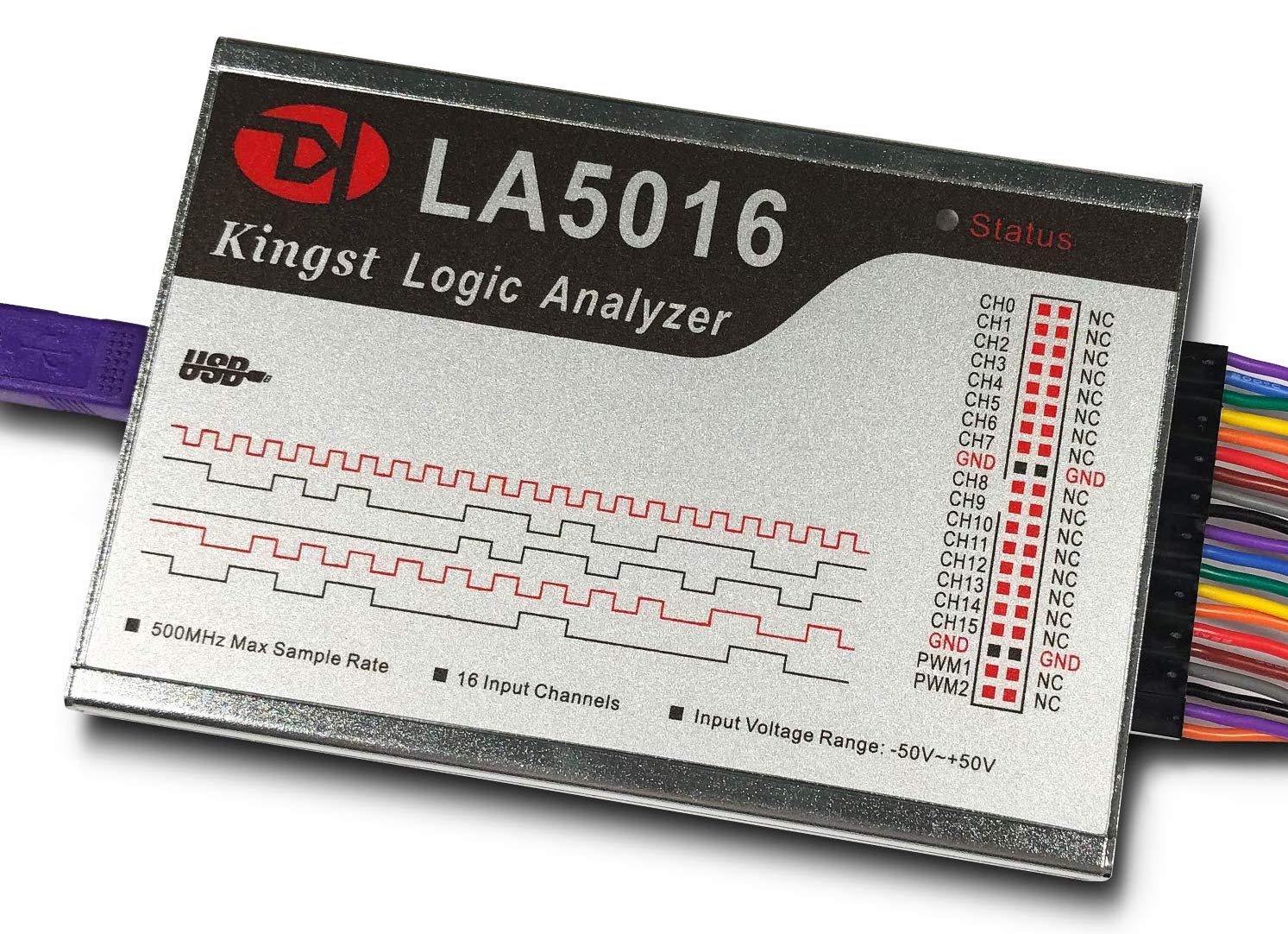
Input Circuitry – For the best signal integrity, each test lead should be a shielded wire with independent signal and ground connectors. An unshielded signal wire and a shared ground connector may be OK for sampling slower signals. The input impedance and capacitance are also important to know. A high impedance and low capacitance are desirable, and will reduce the chances that connecting the LA’s test leads will disturb your circuit. For example the Saleae Logic Pro 16 has a 2 megaohm input impedance and 10 pF capacitance, while the Innomaker LA5016 has 220 kOhm impedance and 12 pF capacitance. Some cheaper logic analyzers don’t even specify these numbers, which is a clue that they’re probably not good numbers. Other input specs to watch for are the minimum and maximum safe input voltages, input protection, and selectable thresholds for logic levels.
Analog Channels and Other Features – One extra feature that’s really handy is analog recording. It’s not going to replace your oscilloscope, but sometimes it’s handy to have a low-bandwidth analog view of your signals that’s integrated with the digital view. The Saleae Logic Pro series offers analog recording on all channels at 50 MS/s and 5 MHz max bandwidth. Initially I thought that was a silly feature, but I’ve found that it’s often helpful for troubleshooting signal contention or logic level problems. Another extra that may be useful is an external clock input, to synchronize samples with a microprocessor clock or other synchronous device. I used to think this was a very important feature, even though many logic analyzers omit it. But in truth, over many years of development I have almost never used it. Some logic analyzers also offer features like programmable digital outputs and other goodies. Whether these are valuable to you depends on your application.
Software – Great hardware isn’t very useful unless it’s coupled with great software for controlling the device and analyzing the recorded sample data. Ideally you want to see lots of protocol analyzers for automatically decoding and annotating sample data for common standards like SPI and I2C. It’s also helpful to have robust trigger support, with multi-stage triggers and triggers based on protocol analyzer results. The software should also make it easy to view, zoom, and measure the recorded sample data.
Price – Logic analyzers can range in prince from about $10 to $1000 or more. The $10 devices can be perfectly adequate for many uses. Fancier equipment may offer many more features, but is it worth the extra cost?
At BMOW Labs
I currently alternate between two different logic analyzers: a Saleae Logic Pro 8, and a no-name 16 channel device. Both are streaming logic analyzers. I think the no-name device is a clone of the Logic 16 (not to be confused with the much more capable Logic Pro 16). Each of these logic analyzers is useful in different situations. The Logic Pro 8 supports fast sample rates around 100 MS/s or better with all channels, and supports analog recording too. But eight channels is limiting, and one of the channels is broken, so the 7-channel device is often not enough.
The no-name device has 16 channels, but no analog, and the sample rate stinks. In theory it supports 100 MS/s with 3 channels, or 16 MS/s with all 16 channels. But in practice I can never get anywhere near those rates before the software gives me an error saying it can’t keep up with this data rate. With 12 or 16 channels, I usually can’t get any better than about 2-3 MS/s before running into data rate errors. I’m not sure if this is because I’ve saturated the USB 2 connection, or because my reasonably-powerful computer can’t keep up, or something else. I’m very curious to know if other people with similar no-name 16 channel logic analyzers have the same experience. The device I have is similar to this one. My back of the envelope math says USB 2 supports 480 Mbps, divided by 16 channels should allow for 30 Mbps per channel, so even when allowing for USB overhead I should be seeing much better performance than I’m getting.
So I’m searching for a logic analyzer with 16 channels, supporting sample rates of least 50-100 MS/s when all channels are used simultaneously, ideally with analog capability, and with decent software. Here are some options I identified:
Some links below may be affiliate links. BMOW may get paid if you buy something or take an action after clicking one of these.
| Saleae Logic Pro 16 | Innomaker LA2016 | Innomaker LA5016 | DSLogic Plus | DSLogic U3Pro16 | |
| Sampling Method | streaming | buffered | buffered | buffered, streaming | buffered, streaming |
| Sample Rate with 16 channels | 100 MS/s | 200 MS/s | 500 MS/s | 100 MS/s, 20 MS/s | 500 MS/s, 125 MS/s |
| Bandwidth | 100 MHz | 40 MHz | 80 MHz | ?? | ?? |
| Min Pulse Width | ?? | 12.5 ns | 6.25 ns | 5 ns | 2 ns |
| Sample Depth per Channel (uncompressed) | unlimited | 50 MS | 100 MS | 16 MS, 16 GS | 128 MS, 16 GS |
| Test Leads | unshielded, independent grounds |
unshielded, common ground |
unshielded, common ground |
shielded, independent ground |
shielded, independent ground |
| Input Impedance | 2 Megohm 10 pF | 220 kOhm 12 pF | 220 kOhm 12 pF | 250 kOhm 13 pF | 250 kOhm 13 pF |
| Voltage Range | -25V to +25V | -50V to +50V | -50V to +50V | -30V to +30V | -30V to +30V |
| Other | analog on all channels | 2 PWM outputs | 2 PWM outputs | external clock input | external clock input |
| Software | simple triggers | simple triggers | simple triggers | complex triggers | complex triggers |
| Price | $1000 | $200 | $300 | $150 | $300 |
It’s tough to pick any clear winners here, but the Logic Pro 16 seems to occupy a category by itself. It’s the only all-streaming device, supporting unlimited sample depths, which is great so long as you don’t encounter unexplained data rate errors. It’s the only device with analog capability, which I’ve found to be a surprisingly useful feature. Its input impedance and bandwidth are the best of this bunch. Saleae’s software and support are have a good reputation, and the overall hardware build quality is very good. The only real drawbacks are somewhat lower maximum sample rate with 16 channels, weaker trigger options, and a much higher price than the alternatives.
The Innokmaker devices are popular and earn mostly good reviews for the hardware and software. They offer options with different sample rates and sample depths at different prices, so you can choose the one that works best for you. I have some reservations about the sample depth. With 50 megasamples per channel (uncompressed) on the LA2016, 200 MS/s recording would fill up the buffer in just 250 ms. That’s definitely too short to accommodate the way I’m accustomed to working. If compression could stretch this to a few seconds, it might be enough, but that’s something that can’t really be evaluated until you try it. The LA5016 offers twice the sample depth, but it’s still not a lot.
The DSLogic devices can operate in buffered or streaming mode, and may have a leg up over the Innomaker competition. In buffered mode, their hardware specs are roughly similar to the Innomaker devices, with the specs appearing to scale by price in a reasonable way. But they also offer a streaming mode option, to achieve modestly longer duration recordings. For unknown reasons, the streaming mode doesn’t provide unlimited sample depth like the Saleae, but is limited to a total maximum depth of 16 GS per channel. While not unlimited, that’s enough for very long captures even at the highest sample rates. DSLogic also provides shielded test leads with independent grounds, and supports more complex triggers than some of the other devices here.
One knock against DSLogic concerns the company rather than the devices themselves. Their DSView software is based on the sigrok open source project, and early versions of the software reportedly used the sigrok code without attribution and without making the derived code public. This has now been resolved, but there’s a lingering sense that DSLogic is not playing fair and there’s some friction between them and the sigrok developers.
BMOW’s Choice
For my own purposes, I think I can limit the options to the Saleae Logic Pro 16 and the DSLogic U3Pro16. The LA2016 and DSLogic Pro are good values for the price, but I think I’d prefer to pay a little more for faster sample rates and greater sample depths. The LA5016 is very similar to U3Pro16, and they’re the same price, but the U3Pro16 is slightly better in nearly every category. That leaves just two contenders for the prize.
Do I want to spend more than 3x as much for the Saleae to get analog capability and a better corporate reputation? The DSLogic has arguably better test leads, and better sampling rates in both streaming and buffered modes, although its input circuitry is probably worse. It’s a tough call. If I were spending somebody else’s money, I would probably chose the Saleae. But when it’s my own dollar, the magnitude of the price difference is hard to swallow.
Read 9 comments and join the conversationMore AVR ICSP Footprints
I’m continuing to research options for alternative programming headers for AVR microcontrollers, building on the ideas I discussed earlier. For one-time programming purposes, the standard 3 x 2 pin 0.1 inch header is just… too big. I’m on the hunt for something that’s smaller, and that can be used on a bare footprint without actually soldering a header. The mockup above shows a 1.5 x 1.5 inch board with the options I’m considering, along with size references from a 32-pin AVR, an 0805 resistor, and a through-hole resistor.
A – The standard 3 x 2 footprint for 0.1 inch pin header.
B – 3 x 2 pin 0.1 inch footprint with zig-zag or lock hole spacing. This helps temporarily hold a header in place through friction.
C – 3 x 2 footprint for 0.05 inch pin header. It’s a lot smaller, but the hole spacing is tiny.
D – 3 x 2 pin footprint with zig-zag spacing for 0.05 inch pin header.
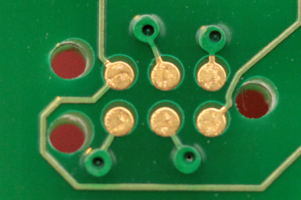
E – 3 x 2 pin footprint for pogo pins with 0.05 inch spacing. It’s nearly the same as C, except the drill holes are smaller. It’s designed for something like the Pogo Key, where the tips of pogo pins snap into the holes, but unlike C the pins don’t actually pass through the holes.
F – An alternative footprint for E. Two positions are holes to help align and stabilize the Pogo Key, and the other four positions are one-sided pads, so more of the PCB’s bottom side is available for other traces and components.
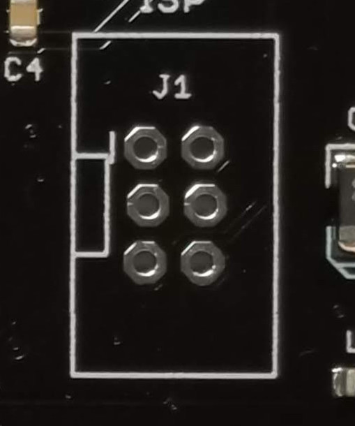
G – 6 x 1 pin footprint for pogo pins with 0.05 inch spacing, inspired by the Pogo ISP Micro. It’s essentially a Pogo Key with a linear layout instead of rectangular.
H – An alternative footprint for G. Two positions are holes to help align and stabilize the pogo pin adapter, and the other four positions are one-sided pads, so more of the PCB’s bottom side is available for other traces and components.
I – 6 x 1 pin footprint with zig-zag spacing for 0.05 inch pin header. Example
J – An alternative footprint for I. The six pins are split into groups of four and two, to prevent backwards insertion of the header.
K – Tag-Connect 6-pin no-legs version.
Here’s a look at the bottom side of the board. No surprises here, but just a visual reminder that the footprints using pads leave more empty space on the bottom for other purposes than the footprints using holes.
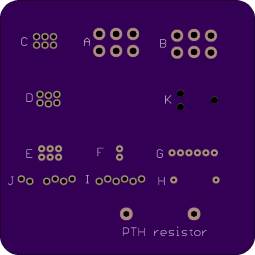
Is using pads better than using holes? I’m not sure. Pads leave the PCB’s bottom more open, but the signal routing for pads may require extra vias for switching between layers that wouldn’t be needed for holes, so it’s not a clear win. Holes also provide something for pogo pins to grip, and are the only way to use 0.05 inch header pins.
Is 0.05 inch spacing clearly better than 0.1 inch spacing? The footprints based on 0.05 inch spacing are obviously smaller, but the holes/pads are so closely spaced that there’s no room to squeeze a trace between them. The larger 0.1 inch spaced footprint is permeable to unrelated signal routing, so although it’s large, it’s not always a major impediment to board layout. The 0.05 inch spaced footprints are like walls that blocks all other signal traces.
I also see a risk of accidentally shorting neighboring holes/pads with the 0.05 inch spaced footprints. The copper of one is only about 10 mils away from its neighbor. If the programmer pins are slightly misaligned as they are lowered onto the board, a pin could land in the empty space between two holes/pads and cause a brief short circuit.
Are 6 x 1 linear footprints better than 3 x 2 rectangular ones? This is hard to answer. They’re the same total area. My first intuition was that 6 x 1 would be easier to fit into otherwise wasted space around the edges of the board. But after looking at it visually, I have an easier time imagining tucking that 3 x 2 into an unused spot than the 6 x 1.
And a Word About Tag Connect
Several people replied to my earlier post to say they’re happily using the Tag Connect cable. From what I’ve read elsewhere, they seem to have a loyal following. Its footprint K is arguably among the best of the options shown here. Yet I’ve almost totally ruled out the Tag Connect, for a reason that you might find silly.
The problem I have with Tag Connect is that it’s a cable and a pogo pin holder combined into a single unit. It’s designed to replace the existing cable on your AVR programmer, rather than attach to the end of the cable as with the other options discussed here. That means you have to purchase different versions of the Tag Connect cable depending on what programmer you have – one version fits the AVR ISP mkII, another fits the Atmel ICE, etc. If you’ve got a USBasp programmer, you’re out of luck, or will have to design your own adapter.
I own both an AVR ISP mkII and an Atmel ICE, so in theory I’d need to buy two different Tag Connect cables. If I wanted to have something assembled and programmed by a third party, I’d also have to worry about what model of programmer they have and whether a Tag Connect cable exists for it. The result would be a lot of hassle and equipment duplication, compared to any of the other options, where I could just snap an adapter onto the end of the existing programming cable.
Perhaps I could design my own adapter board for the generic Tag Connect cable, so any programmer’s 3 x 2 pin female header could plug into my adapter, and Tag Connect’s 3 x 2 pin female header could plug into another socket on the adapter. But this would result in twice the total cable length, which might impact signal quality and reduce the maximum possible bit rate for programming. Edit: I see that Tag Connect sells an adapter board like this for other MCUs, so maybe it’s fine and signal degradation isn’t a problem.
If Tag Connect sold something similar to the Pogo Key but with alignment pins, it would be a great option. But as things stand with the integrated cable, it complicates programming for anybody with multiple different programmers or who contracts third party programming with unknown programmer hardware.
Read 9 comments and join the conversationAlternative AVR Programming Header Ideas
That ubiquitous six pin header for in-circuit programming of Atmel AVR microcontrollers – it’s the standard, but it’s not a great standard where size and cost are a concern. Can I do better?
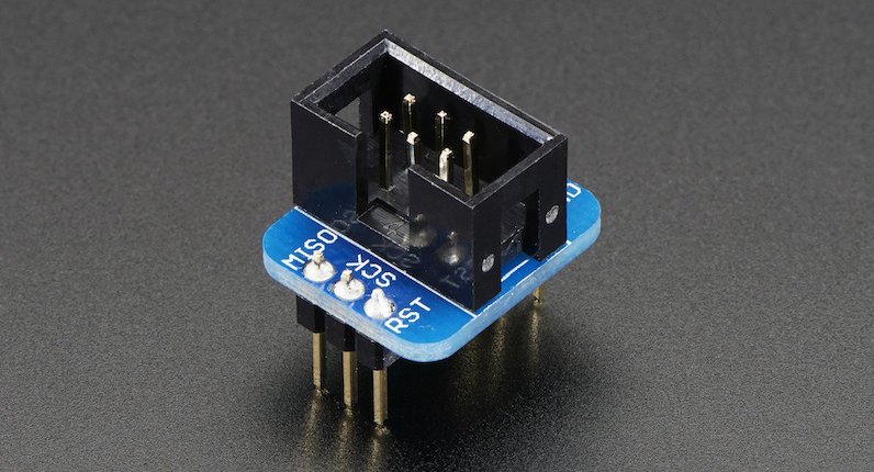
Programming most AVRs requires a six wire interface, with a clock, serial in, serial out, reset, power, and ground. It’s common to include a 3 x 2 pin 0.1 inch header on any AVR-based board. Typically a keyed box header is used to prevent accidental backwards cable attachment, like the header on the Adarfruit breakout board shown above, but sometimes bare 3 x 2 pin 0.1 inch headers are used.
That’s fine for hobbyist work or building a prototype, but when building larger numbers of AVR-based boards, the 3 x 2 pin 0.1 inch header has two significant drawbacks. The first is the component cost and related assembly cost for a header that will only ever be used once, for a few seconds during manufacturing. It’s not a huge cost, but it’s still a factor when trying to minimize the cost per unit – why throw away money? The second drawback is the relatively large physical size of the 3 x 2 pin 0.1 inch connector. For small boards containing mostly surface mounted parts, the ICSP header can complicate layout and routing, or require enlarging the PCB.
Ideally we want a programming connector with these attributes:
- zero per-unit cost
- small footprint, preferably one-sided
- keyed to prevent backwards cable connections
- holds cable firmly attached to the board
Here are some options to consider.
Empty Footprint 0.1 inch
The simplest option is keep the standard 3 x 2 pin 0.1 inch header footprint, but don’t actually solder a header into it. When it’s time to do programming, place a 3 x 2 header in the holes, and apply some sideways finger pressure to ensure the pins make solid contact with the hole plating. It’s low tech, but it works.
A small optimization is to use a 3 x 2 pin 0.1 inch lock header footprint, where the holes for the individual pins are very slightly offset instead of appearing in a perfect grid. This helps hold the header in place temporarily with friction, so finger pressure normally isn’t needed. It’s what I do for Floppy Emu programming, as shown here:
This approach eliminates the cost of an otherwise-useless programming header, but it’s still too big and doesn’t prevent backwards insertion. And even with the lock header footprint, it’s not great at holding the cable in place for extended periods of development or debugging. The pins often slide out of the holes.
Empty Footprint 0.05 inch
A second option is to use an empty 0.05 inch header footprint, which reduces the required board area to just 25% of original. That’s great, and this might be a good solution. But most AVR programmers have a 0.1 inch cable, so a 0.1 inch to 0.05 inch adapter will need to be built or purchased. That’s a minor drawback, but it only needs to be done once.
0.05 inch pin headers are fairly delicate. Would they hold up to hundreds of insertions and removals, with the added forces of finger pressure or lock headers?
This solution is also not keyed to prevent backwards cable insertion, nor does it grip the cable tightly.
Empty Non-Rectangular Footprint 0.05 inch
If I’m contemplating building a 0.1 inch to 0.05 inch adapter anyway, there’s no reason the 0.05 inch end needs to retain the standard 3 x 2 layout. I could do something with 4 pins in one row and 2 pins in a second row, or any other kind of irregular pin spacing that would prevent backwards cable insertion. Maybe a 7 pin single row design, with one of the pins removed. This would make the footprint area slightly larger than a 3 x 2 layout, but it might be worth it to prevent accidental backwards connections.
Pogo Pins
Any kind of footprint with plated-through holes will hinder routing and component placement on both sides of the board. Spring-loaded pogo pins provide an alternative approach, making it possible to build a one-sided programming interface with exposed pads, similar to this:
With 0.05 inch spaced pogo pins this allows for the smallest footprint of all, but the pogo pins need to be held against the board with one hand during programming, making it awkward to use. It’s OK for a programming operation lasting a few seconds, but not for anything longer.
This simple AVR ICSP pogo pin adapter from Tindie shows one such approach:
It’s nice, but there’s nothing to help align the cable or prevent backwards connections.
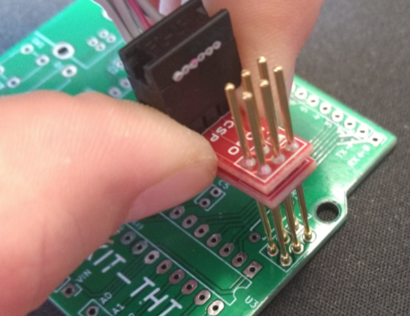
For a fancier solution, there are pogo pin cables from Tag-Connect that include alignment pins and optional locking legs to hold the cable firmly on the board:
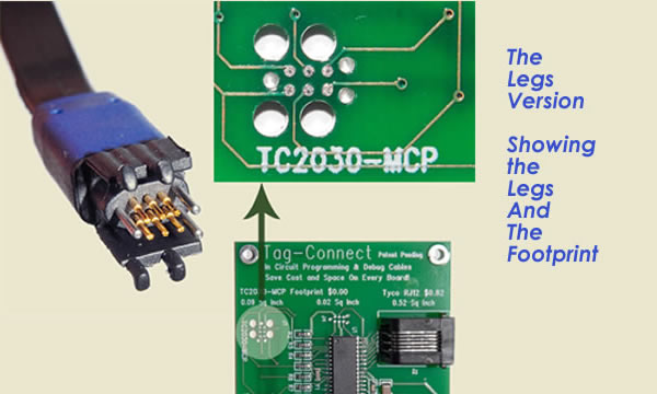
But when you include the area needed for the alignment pin holes, the Tag-Connect footprint is essentially the same area as the standard 3 x 2 pin 0.1 inch header footprint, and the size advantage is lost. And with the version of the Tag-Connect cable that has locking legs, the required footprint area is even larger. Look at this beast:

Conclusion
So what’s the best option? I don’t think any of them is a clear winner – they all have advantages and disadvantages. I really like the idea of pogo pins and exposed PCB pads, but the required alignment pin holes mostly negate the space savings, and I don’t like the idea of always needing one hand to hold the cable in place. For my purposes, I think the non-rectangular footprint with 0.05 inch headers is worth exploring further. I’ll see what I can cobble together for testing.
Read 12 comments and join the conversationPCB Autorouting
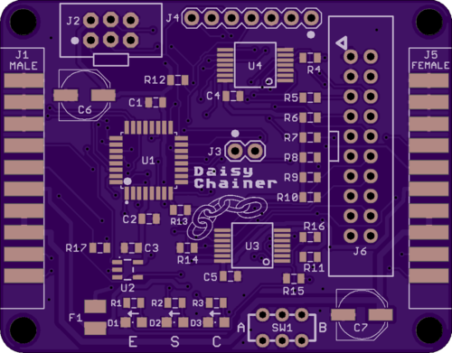
The Apple II Daisy Chainer for Floppy Emu is done, and I’ve ordered a few PCBs made for testing. This proved to be a surprisingly challenging board to lay out and route the traces. It’s a simple two-layer board, and I wanted to keep it as small as possible, so the signal routing quickly became very congested. Hand-routing of the first 40 traces took almost a whole day of tedious work, so I finally gave up and tried autorouting the remaining 80 traces. And it worked! The result looked pretty good, too. I’m curious to know how autorouting has turned out for other hobbyists. Have you ever autorouted nearly an entire board? What were the results?
I haven’t had good results with Eagle’s built-in autorouter, so for recent projects I’ve been using a stand-alone autorouting software package called Freerouting. It’s a Java-based app with a slightly awkward UI, but it’s impressively powerful. First you export your Eagle board file in .DSN format, using a script provided by Freerouting. Then you import the DSN file into Freerouting and let it work, running for about 1 to 15 minutes. When it’s finished you can export an Eagle session script, which will rip up all your old tracks and lay down the new ones calculated by Freerouting.
Obtaining good autorouting results requires careful setup of Eagle’s design rules. For example, the default might be to use 8 mil traces with 8 mil minimum spacing between traces, but power and ground might be treated as a separate net class requiring 20 mil traces for extra current-carrying capacity. The design rules also define what size drill to use for vias, and how close to the edge of the board it’s OK to route traces. The autorouter takes all of these constraints into account when it does its job.
So what’s not to like about the autorouter? Can a skilled human do a better routing job? Why not autoroute everything? Here are a few drawbacks that I found.
Fixed Component Placement – When I route by hand, I’ll sometimes discover that I’ve placed a component in the middle of a chokepoint for PCB traces. If the placement isn’t critical, I can move the component to make routing easier. The autorouter can’t do this, at least not that I’ve seen. It treats the component placements as fixed and immutable, even when nudging a resistor 10 mils to one side could make a huge difference.
In theory there’s no reason that the autorouter couldn’t handle changing component placements. Additional constraint information could be supplied, providing a bounding box of acceptable placements for each component, or tagging some component placements as critical and non-movable.
Unnecessarily Aggressive Routing – If the design rules say that 8 mils is the minimum acceptable spacing between traces, the autorouter will often stack traces 8 mils apart even when there’s plenty of room for wider spacing. It’s too aggressive – pushing spacing to the limit when it doesn’t need to. In theory this shouldn’t be a problem, but it feels like poor design practice to me. To avoid the risk of accidental short circuits, I prefer not to push the PCB manufacturing limits except in those few areas of the board where there’s no alternative.
A good example is autorouting between adjacent pins of a 0.1 inch header. There’s roughly 30 mils of space between the metal rings that surround adjacent pins, providing enough space for an 8 mil trace with 11 mils of space on both sides. But Freerouting often placed such traces off-center, with 8 mils of space on one side and 14 on the other. It met the design rules, so from its viewpoint there was no reason not to do it that way.
In practice an 8 mil minimum spacing is already conservative, and most PCB manufacturers can do 6, 5, or 4 mil minimum spacing. So it’s unlikely this behavior will cause any trouble here, but it might for other boards with smaller minimum spacings.
Nuances of the “Best” Routing – Once Freerouting finds a routing solution, it tries to optimize it by minimizing the total trace length and the number of vias. These are good optimizations, but sometimes I want other considerations to trump them. For example when I route manually, I try very hard to minimize vias in power and ground traces. I would be happy to add 5 extra vias elsewhere if I could eliminate one via for power or ground. Freerouting doesn’t support this kind of trade-off, so all vias are treated equally.
A related consideration is the number of power and ground paths. The autorouter considers a pin to be powered if there’s any combination of traces leading from the power supply to the pin. Only one such path is required, and the result is a logical tree with the supply at its root and the power pins at the end of the branches. But when I route manually, I often connect branches back together, creating multiple paths from the power supply to the pin. I use the same approach for grounds. The goal is to minimize the voltage difference between power and ground points on different regions of the board.
The autorouter doesn’t care about visual aesthetics, and normally I don’t either. But when two possible routes are equally effective, I normally choose the one that’s similar to other traces I’ve already routed. It makes the board’s interconnections easier to understand at a glance.
Freerouting also doesn’t account for any potential analog signal effects, at least not that I’ve seen. If it’s important to minimize the trace length for a specific signal, or match the trace lengths of two signals, it can’t help. It also doesn’t consider problems like the parasitic capacitance formed by two long parallel traces. Depending on the signals, the signal speed, and other factors, a skilled human might choose to route two signals on non-parallel paths even if parallel routing was the shortest distance with the fewest vias.
Do you have any autorouting secrets to share? Let’s hear them!
Read 8 comments and join the conversationAtmel ICE Wiring Horror
The Atmel ICE programmer/debugger has its SWD connector pins reversed from the standard ARM Cortex debug connector. Arghh… why? It’s the same physical connector (5×2 0.05 inch polarized male), but the pins are rotated 180 degrees from the standard, as if the cable were plugged in backwards. Incredibly, it also ships with a 180-degree reversing cable, so it works – as long as you use their cable. It’s not a mistake: the product is actually designed around a reversed connector with an un-reversing cable.

WHO BUILDS A PRODUCT THIS WAY?? I shake my fist at you, Atmel hardware designer. This is like designing an electric outlet where 110V and ground are swapped from their normal locations, but bundling it with an appliance cord that unswaps them.
The problem began when I grew tired of Atmel’s tiny 4-inch cable, and decided to get a replacement cable. Naturally I used a standard 10-pin ribbon cable with 5×2 0.05 inch connectors on each end: Adafruit’s purpose-made SWD cable for ARM development. I couldn’t understand why it didn’t work, and why strange things happened when it was plugged in.
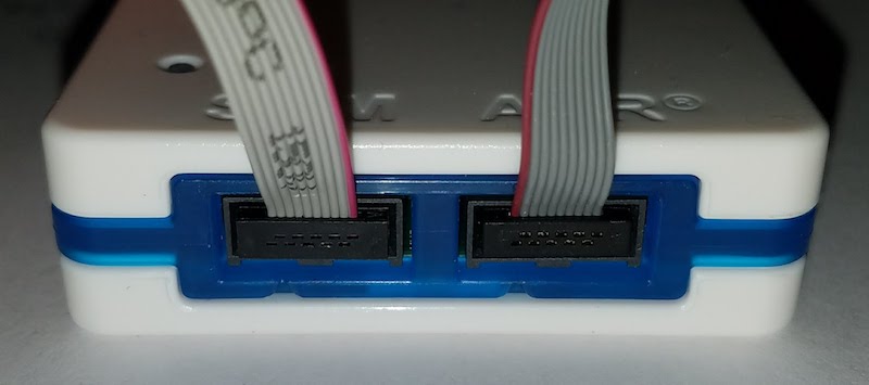
After scratching my head for a while, I noticed something odd. The title photo shows both the original cable and the Adafruit cable connected to the Atmel ICE. Notice how one has the red stripe on the right, and the other on the left? Ouch!
From looking at the original Atmel cable, it’s not at all obvious that the pins are reversed. It looks like a straight-through cable, because each connector is crimped straight on to the 10-pin ribbon, with no crossing wires. But a more careful inspection reveals that one of the connectors is crimped on so it’s facing the opposite direction of the other, resulting in a 180-degree rotation of the pin assignments. It violates the rule of the cable’s red wire indicating the location of pin 1. (Ignore the extra 6-pin header, which is used for other devices)
The good news is that there’s no permanent damage to my ARM board. The bad news is that I still need a replacement cable, but now I need to build a reversing one.
Read 18 comments and join the conversationCrazy Fast PCB Manufacturing
I finished the redesign for my Apple IIc Drive Switcher PCB on Monday morning, and submitted the Gerber files to Elecrow on Monday at 11:25 am. Friday at 5:20 pm I held the finished PCBs in my hands. Only 4 days for manufacturing and delivery. From China. According to the tracking info, my package took just 17 hours to travel from Elecrow’s Shenzhen facility to my doorstep in California. Total cost for everything was a mere $29.96.
We live in a crazy world, where a completely custom and intricate item can be manufactured on the other side of the planet and delivered to my door in 4 days, for the cost of a pizza and beer. Thank you Elecrow!
Read 1 comment and join the conversation