

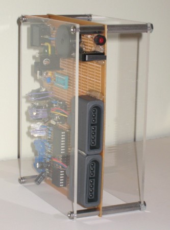
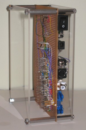
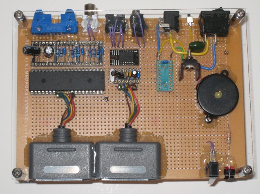
Uzebox, Take 2
It’s done. Yes, it cost twice as much money and 100X as much time as just buying one from Adafruit or Sparkfun, but I’ve finished my home-made Uzebox.
Notable features vs. the “stock” Uzebox:
- vertical mount
- mini-stereo jack for audio
- internal speaker
- transparent acrylic case
- lots of glue
And it plays Arkanoid! Now I can return to my regularly scheduled life. 🙂
I wrote about the Uzebox earlier: it’s an open-source hardware project utilizing a microcontroller to synthesize an NTSC video signal on the fly, in software. Many classic games have been ported to it, and there’s an active developer community.
Read 11 comments and join the conversation11 Comments so far
Leave a reply. For customer support issues, please use the Customer Support link instead of writing comments.
I see you did Point to Point soldering. Good luck with that if you ever need to debug it. 😛 (Still shudders thinking of debugging his CPU project if things go amuck… I hate P2P soldering. 😉
Oh, also see you have a favicon on the site now!
It’s actually wire-wrapped between the chips, the programming header, the power rails, and anything else I could get wire-wrap pins for. But the connections to things like the s-video jack and SNES gamepads needed to be soldered.
I saw the photos of your CPU project, and that’s definitely a healthy amount of hand-soldering!
😉 More like unhealthy with all that lead based solder. 😛
*Facepalm* Didn’t look at the picture showing a glimpse of the wirewrap side. I think it’s time for me to go to bed. 😛
(Notes an excessive use of smilies. Indeed, it is time to go to bed.)
New solder is not lead-based anymore, is it?
There’s an EU directive that took effect in 2006 that prohibits it in pretty much all electronics and since 1) the European Economic Area (*) is huge (bigger than the US), all electronics manufacturers in the world have had to comply and 2) the EU is the world’s most important regulator. The rest of the world usually follows EU regulations about such things as food additives, hazardous materials, etc.
There’s an article about in the Economist (behind a paywall):
http://www.economist.com/world/europe/displaystory.cfm?story_id=9832900
Somebody copied the whole thing here (scroll down to “How the European Union is becoming the world’s chief regulator”):
http://www.thenhf.com/codex/codex_84.htm
According to wikipedia, California law includes the EU directive by reference.
—
*) The European Economic Area is the EU + the remaining few EFTA countries (Iceland, Norway, Liecthenstein), except for Switzerland. Almost all EU directives apply there even though Iceland/Norway/Liechtenstein have no representation in the commision, council, or parliament.
Brandon, you should really make your own PCBs. It is really not that hard. Here’s how I do it:
I bought a small fluorescent light (mount, tube, transformer — the whole thing) for about 100 DKK (*). Then I bought a UV-tube that fit for about 200 DKK. I got an A4-sized thin piece of glass at a local picture framer for 20DKK (he even smoothed out the edges for me so I wouldn’t cut myself). I marked all the edges in red with a permanent marker for safety.
I use standard precoated photo-sensitive PCBs — you can coat your own with a spray but it doesn’t seem to be worth it.
I use EagleCAD for drawing the circuit and laying it out (it can pretty much do that automatically) and print it out on my trusty HP LaserJet 1022. It’s got a 1200 DPI resolution which allows you to make 6 mil traces — or even 4 mil if you optimize the whole process well enough. In other words, pretty much any printer will do. EagleCAD works under both Windows and Linux and is free for small single and double-sided prints. The UI is nothing to write home about but it’s workable.
You can use standard white A4 office paper — or whatever barbaric sizes you use over there 😉 — but the results are not good because it contains chalk/clay which blocks much of the UV light. You can improve things a bit by making the paper wet with water or oil or you can remove it chemically (I tried it, you really can) but it’s better to use a different kind of paper. I use a bit of thing drafting paper taped to an A4 piece of paper as carrier.
Peel off the light protection from the photo PCB. Put the drafting paper on top (toner side down). Put the glass pane on top. Then put the light fixture on top of the glass. You don’t even have to place it all that carefully or use a smart light reflector or a collimating structure. A single UV tube placed just about at random works quite well. Place a cover of some sorts above the whole thing (for eye protection) and turn on the UV tube for about 90s. Please be as paranoic as possible regarding UV light and your eyes!
As long as you do all this indoors and aren’t extremely slow, you don’t really have to worry about light damage. (I tested this using both sunlight and direct light from various types of lamps I had. The photo resist is pretty much only sensitive to UV light. You could lay the unprotected photo PCB directly under a lamp for an hour with no problem at all.)
The next step is to develop the board, that is, to get rid of the photo sensitive coating that didn’t get any UV light (or the parts that did — it depends on whether you use negative or positive boards).
I use standard drain cleaner (a strong KOH solution) + standard tap water in a flat plastic container for about 10s. You should be able to clearly see a colour change (to a very deep red) when it’s time to stop. Then you rinse it in running water until you gotten completely rid of the KOH.
Do not overdevelop. The hardened part of the resist is not immune to the KOH base, it is just more resistent, so if you overdevelop you end up removing all the resist.
Other photosensitive solutions will behave differently and might not turn red. Also, the developing time depends on the strength of the KOH solution. NaH supposedly works just as well. You can add a fixing agent that makes the developing stop (or drastically slow down) when it’s done. This should make things more idiot proof but I never bothered with it. Timing + the visual change works well enough for me.
KOH is pretty safe. The Swedes have “delicacy” where they steep a fish in KOH and then rinse it carefully with water. Just make sure you don’t get it in your eyes (use glasses) and make sure to clean your hands afterwards. KOH (and NaOH) turns fat into soap so if you get some on your hands, you do want to get it off quick (use more soap + oil or skin cream).
Now you have a nice developed board but you still need to etch off a lot of the copper. The old way was to use FeCl but that’s pretty nasty (and colours everything brown — if you get it on your fingers they will stay brown for a long time). The modern way is to use Sodium persulfate (aka “Feinätzkristall” in German, sold as Seno 3207). I put a bit of that powder + some warm water (about 50°C) in a clear plastic freezer bag together with the board. I tie a good(!) knot on the bag and put it into a warm water bath (about 50°C). I occasionally pick up the bag and shake it and put it into that bath again.
The etching solution works best at about 50°C so don’t get it too hot.
You can reuse the etching solution for several boards, until it has changed from the original clear to windex blue. But be careful about how you store it! It is probably better to just throw it out when you are done. If you pour it down the drain, make sure to add lots of water to dilute it.
You can use lots of other etching agents (HCl works fine, too) but Feinätzkristall is the easiest and nicest that I know of.
Rinse the finished board under the tap — and you are done! I haven’t found it necessary to use a coating to protect against corrosion but other people swear it’s necessary. Your mileage may vary.
You can often design the board to minimize (or eliminate) holes (old-style TTL chips can be surface mounted if you bend the leads). But if you want to drill holes, get the right bits. A drill stand is not strictly necessary but you do end up breaking much fewer bits…
Use old clothes so you don’t end up with holes in a pair of trousers you like.
The whole process, from clicking “OK” in EagleCAD’s print dialog to the finished dry PCB takes about 15 minutes (and it could be reduced to about 5 if I bothered to optimize the development and etching a bit).
I experimented with about 50 small pieces (0.5cm x 0.5cm) of photo PCB while I tuned the process to my liking. Tin scissors work fine for cutting up PCBs. If you cut a PCB, then smooth out the edges with sanding paper before you place it under the glass for exposure. You want the drafting paper with the layout to be as close to the resist as possible and an uneven PCB edge really ruins the whole thing.
If you use sanding paper or drill holes, please protect your nose and mouth. The dust is not particularly healthy.
—
*) 100 DKK is about 20$ (and we have a 25% sales tax here in Denmark so it should work out to much less than 20$ for you).
Wow, that wins the award for longest comment ever. 🙂
That’s pretty impressive that you can turn out a new board in 15 minutes. How expensive are the raw copper-clad boards?
With a single-sided board, and no holes, it seems you’d be limited to fairly simple designs. Although you could solder a jumper wire if you needed one trace to cross another.
Mail-order custom PCBs have also gotten pretty inexpensive. You can get small two-sided PCBs made for about $30, with all the holes and plating and everything else. If you know exactly what you want to build, I think it’s a great option. But if you expect to go through many prototype versions, it could quickly get expensive ordering new PCBs for each revision.
They are not particularly expensive (and you can cut them into smaller pieces if you like). Photo PCBs cost a bit more than raw copperclad PCBs but not much more in retail. A single single-sided 10x16cm² photo PCB is
28 DKK in retail. Call it 5$. They will keep for years unless you store them in a particularly stupid way.
Of course, your prices in California (is Belmont considered part of Silicon Valley?) will be vastly different from my prices in Copenhagen. Denmark is not known for low prices…
You can do TTL designs without holes — and the need for two sides is not that high when you can make 6- mil traces: I can get two traces between each lead of a TTL chip. Three, if I’m careful. The bottleneck for the trace width is not the printer or exposure or developing process, it is the etching process. If you look at the cross section of an etched trace you will find that the sides are not at right edges to the board and the top of the trace, rather they are at an angle. It is very hard to get a steep angle there but you should be able to get at least 60 degrees. Since the thickness of the copper is 35 µm, it is hard to get below 4mil in width without also etching off a bit of the top of the trace. The professionals use something that shapes the solvent flow in the boundary layer in order to make the sides as steep as possible — but I just shake a freezer bag 😉
Btw you can do dual-sided PCBs yourself, too. It adds about 2 minutes because you need to expose both sides — and because you need to line them up carefully. A trick is to align the two pieces of paper carefully by hand and then staple them together so they form a stable pocket.
I do have a drill. I got a dremel drill with stand for about 1000 DKK (tools are a bit expensive here and there’s that pesky 25% sales tax).
Plating is rarely necessary — and if you need to enlarge the cross section in order to reduce the resistance on your +5V and GND, then it’s very easy to add solder to the relevant traces. It’s a 5 second job.
So, how about giving homemade PCBs a try? I guarantee you will love the turnaround time 🙂
If you want to do it on the cheap first, then use the midday sun outside as your UV source, forgo the glass cover (use paper clips instead), use diluted draino as the developer (I think — but the Aluminum might cause trouble), and use HCl (muric acid) as the etcher.
It’s not as easy that way, the quality is not as good, and you’ll have to be more careful but it certainly is possible.
I do recommend the UV tube, the glass plate, drafting paper, KOH without Aluminum, freezer bags, a dedicated flat plastic tray, a dedicated plastic container for the water bath, and some Feinätzkristall (Fine Etch Crystal), however.
Depending on where you live the water company might not like you pouring sodium persulfate down the drain. 🙂
I think the dissolved copper is the worst problem but you will have that with any etchant (unless you regenerate it by extracting the copper).
And Bordeaux mixture, a copper-based fungicide, is still in use.
Heavily diluted etchant shouldn’t cause problems in the pipes or with the microorganisms used at the wastewater treatment plant — think of sodium hypochlorite or draino, which we do pour down the drain without hesitation.
But yes, please follow the local rules for waste disposal. I did some experiments with accelerant additives (a bit of iron and some soap and some other stuff) which I’m carefully keeping stoed until I can be assed to go to the friendly neighbourhood hazmat depot.
Well about all I can add is “NICE!”.