

FPGAngst
I’ve spent the past few days getting familiar with my Xilinx Spartan 3A Starter Kit, and so far, it’s not going well. I’d thought I was pretty competent with the basics of digital electronics, and the concepts of HDL programming and FPGAs. But working through a “blink the LED” example using the Xilinx ISE WebPack software has been an exercise in frustration. The learning curve is more like a brick wall, and I’m getting dizzy from banging my head into it over and over.
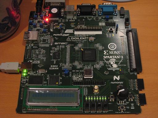
I’ll begin with the starter kit itself. Given the name, you might think it’s aimed at people who want to get started with FPGAs. Forget it. I was very disappointed to find that the starter kit came with almost no documentation at all. Instead, it just had a DVD with a two year old version of the ISE software (now two major releases out of date), and a leaflet with a URL to find more information. The only printed documentation was for the Embedded Devlopment Kit, which is a separate product and doesn’t even work with the free version of the Xilinx ISE. Following the URL, I found the manual for the starter kit, but it’s little more than a catalog of all the hardware on the board. If you want any kind of tutorial for an FPGA “hello world” using this board, or a high-level overview of the various steps involved in creating and programming an FPGA design, or any kind of “starter” information at all, you’ll have to look elsewhere.
Plowing through the ISE software on my own, the first issue I faced was the need to choose what FPGA model I wanted to target. You might think there would be a predefined choice for “Spartan 3A Starter Kit”, but you’d be wrong. After some digging, I found that the starter kit has a XC3S700A, but that wasn’t enough. I needed to specify what package it was, and what speed grade too. How do you tell this? It’s mentioned nowhere in the starter kit manual. After about 20 minutes of searching around, I finally managed to find the web page that deciphered the tiny, near-illegible numbers printed on the chip to determine the package and speed. It’s FG484-4, if you’re keeping score at home.
The ISE itself is really bewildering. It’s basically a shell application that coordinates half a dozen other tools, each of which has its own UI and terminology. The other tools look like old command-line apps that someone slapped together a GUI for using Tcl/Tk. The ISE uses a strange (to me at least) “process” metaphor, which is a context-sensitive subpanel that fills with different actions, depending on what you’ve selected in the main GUI. It took me two days of hunting to figure out what I needed to click on to make the simulation-related process options magically appear. The processes are also arranged in a hierarchical list, so in most cases, running a process requires running all the ones in the tree before it. I still haven’t figured out how to check if my Verilog compiles without doing a complete synthesize, place, and route for the entire design.
Other ISE headaches:
- The GUI-based Plan Ahead tool used to assign signals to physical pins bears no relation to the text-based UCF (user constraints) file examples in the starter kit online manual.
- ISE keeps getting confused about the UCF file, and I have to remove it from the project and re-add it. It’ll complain that I don’t have a UCF file, then when I try to add one, it complains there already is one.
- Integration with iMPACT (the programming tool) is apparently broken. ISE says it’s launching it, but doesn’t. iMPACT must be launched manually.
- After using a wizard to create a DCM module to divide the input clock by two, there’s no “results” page or other info that defines what ports the wizard-created module has. It doesn’t let you actually look at the module code: clicking on it just relaunches the wizard. I had to go poke through random files on disk to discover the module ports.
In comparison to the software, the hardware itself seems pretty good, but maybe a little TOO good. There are no less than four different configuration EEPROMs that can be programmed, with a complicated system of jumpers for controlling which one to program and which to use at startup. This just makes life more complicated than it needs to be.
The only big negative about the hardware is that there’s no SRAM at all. I don’t know how I missed this when I was looking at the specs. Instead, it has 64MB of DDR2 SDRAM. Yeah, that’s a lot of RAM, but creating a memory controller interface for DDR2 RAM is a big honking complicated task all in itself. That means that if you want to do any kind of project involving RAM, you either need to be content with the few kilobytes of block RAM in the FPGA itself, or go on a long painful detour to design a DDR2 memory controller first. The 133MHz oscillator for the DDR2 RAM also occupies the only free clock header, so it’s impossible to introduce another clock to the design (for example, a 25.175MHz oscillator for generating VGA video).
Stumbling blindly through the software, I did finally manage to design, simulate, program, and run a simple example that blinked three LEDs. I’m sure everything will make more sense in time, but it’s hard for me not to feel grumpy right now. I feel like I’m spending all my energy wrestling with the tool software, and none on the project itself. In short, it feels like a software project, not a hardware one. I’ve barely touched the board, other than to plug in the USB cable and flip the power switch. My multimeter, chip puller, wire stripper, and other tools sit unused in my toolbox. Instead, I’m spending time reading a lot of manuals and guessing at what some opaque piece of software is actually doing under the hood. The experience with the clock generation wizard was downright depressing: it just writes some HDL code for you and doesn’t even let you see it, so you’re at least two levels removed from having a prayer of actually understanding what’s going on. Since my end goal in all my homebrew hardware is to gain a better understanding of how things work, that’s especially galling.
I’m going to search out some more ISE tutorials and any other good learning tools I can find, but I’m also going to take another look at the Altera tools. I’ve heard that the Altera software is more beginner-friendly, but I went with Xilinx becuase their starter kit appeared more powerful. I’m now realizing that the quality of the software tools and ease of the development experience is much more important than the number of gates on a particular FPGA. Altera’s Cyclone II starter kit isn’t as full-featured as the Xilinx kit I have now, but it’s decent, and it has some SRAM too. More than likely, the Altera tools will just be a different flavor of incomprehensibility, but it’s worth a look.
Read 37 comments and join the conversation37 Comments so far
Leave a reply. For customer support issues, please use the Customer Support link instead of writing comments.
I know your pain… I’ve often thought that if Xilinx were a software company instead of a hardware company, they would have long since gone out of business. My most frustrating experience with ISE was spending a week trying to debug a faulty state machine in a design only to finally discover that the version of ISE I was using had a bug that was causing the logic to get the true and complement outputs of the flip-flops backwards when determining the next state. This bug, of course, lead to state transitions that shouldn’t have been possible.
Normally (unless there’s a new bug), you shouldn’t have to manually go through intermediate process steps. If you try to start some process that needs the result of a prior process, it will use some sort of built-in makefile-like logic to run the intermediate process steps. If I want everything updated, I usually just double-click on “Generate Programming File” in the process tree.
As far as the VGA clock is concerned, you should be able to get one of the DCMs to synthesize the needed frequency from one of the existing clocks.
I’ll look for an example of this in code form, so you can see what’s going on.
Ugh, chasing that state machine bug doesn’t sound fun.
I should have clarified about the clock. I did use the DCM clock wizard to synthesize a video clock, but the closest it could get to 25.175MHz is 25.0MHz. I used 25.0MHz initially for BMOW, and it works, but it forces you to reduce the number of pixels on each line slightly in order to keep the horizontal frequency the same. This causes a sampling problem on LCD monitors, because it samples your video signal 640 times per line, but the color is actually changing something like 634 times per line. This caussed some ugly vertical banding when I tried it for BMOW, which is why I eventually switched to an exact 25.175MHz clock. Maybe there’s some other clever solution I haven’t found yet.
Also, regarding the intermediate process steps, what I meant was that I haven’t found anyway to just compile my Verilog (checking for errors), short of actually running the whole Synthesis step. Or is that all the Synthesis step does? It seems like it also builds a hardware model of muxes and LUTs and flip-flops that looks very impressive when viewed, even if it’s not very useful.
I started learning Verilog not too long ago after Bob, one of the guys at HBRC did a “Hello World” tutorial. Basicly just light up the 8 LEDs on the board. I personally hate ISE and use a Makefile instead. Bob has a guide on using the Xilinx tools from the command line that may be helpful: http://www.demandperipherals.com/docs/CmdLineFPGA.pdf. I’ll come up with a list of books I found useful.
There’s accidental period at the end of that link, just FYI. Check his site for the Makefile.
It took me a few years before I found it – even using ISE every day for work:
To just compile the verilog without running the full synthesis step, there is a “Check Syntax” option under synthesis. Select a source file to check in the sources window and then click on the ‘+’ beside the Synthesize – XST process in the process window. This will open the process tree and you’ll see a “Check Syntax” option. Double click it and it will compile the selected source file. Hope this helps.
ISE has been known to have “quirks”. I’ve found that doing a project cleanup to help (Project->Cleanup Project Files).
As to the DCM clock wizard, it intentionally abstracts the user from the implementation since DCM’s have dozens of settings – the DCM is a hardwired part of the FPGA.
Hello,
I became interested in your project starting with 3DT. I am CS student and just took a course regarding VHDL ( Verilog same thing ). I have some short lab tutorials that would help you with the basics through ISE, unfortunately I can’t find you e-mail address anywhere, so I am writing this here.
You could change the oscillator for another one from which you can generate the required pixel clock. 25.175 MHz and 50.35 MHz oscillator modules are available. Alternatively (but rather messily), you could remove the existing oscillator and connect an external 25.175MHz one to the exposed pad. If you do this, keep the wires really short!
I don’t imagine that under-clocking the RAM would be a problem. You could call it a “feature” as it would lower the power consumption a lot. I daresay there is a built-in PLL you could use to run things faster if you want to.
I’m not very familiar with the XILINX parts, but did tinker with my own microprocessor design on an Altera FPGA, which I also use for work. The PLLs are very handy!
I didn’t like the ISE, either, when I was working with it. Yes, their Processes metaphor sucks. And yes, the real work is done by a bunch of command line tools ported over (badly) from Unix, with some GUI sprinkled on top. Done badly. There are also some batfiles in there to invoke some of the tools, where the argument quoting is done wrong (at least that used to be the case). In other words, you might want to avoid using paths with spaces in them…
I recommend Verilog over VHDL despite the quirks it has and despite the fact that it was clearly designed in several stages by committees of people who don’t know much about computer languages. But VHDL was designed by people who thought ADA was a good idea…
There’s simply much less noise in a Verilog program.
If you want to play with Verilog without the ISE, you can use Icarus Verilog.
(Synthesis reads the files and converts them to combinatorial logic and latches. It tries to minimize the logic and the signal paths between the latches at this point but it doesn’t know the real hardware yet so there’s a limit to what it can do. Place and route maps the logic and latches onto real logic blocks on the FPGA and allocates wires (routing) between them. Sometimes logic has to placed weirdly because there’s not enough wiring available for better placements.
There’s a timing tool that uses the place and route results to find the slowest signal propagation time between latches (and adds the latch times) to generate a timing report. This tells you the fastest speed of your design for each clock domain — and gives you plenty of data for optimizing it. You can force some of your “program” into specific types of logic cells (some are good for driving I/O, for example) or even into specific logic cells at specific places on the chip but that’s a bit like assembly programming and should be done as little as possibly.)
I believe there is a GUI tool that lets you create a DRAM controller with a few clicks. That might prove useful 🙂
Some of the tools that generate code for you contain proprietary information so you aren’t going to get a look at that source code. Sorry.
Places where getting the source code is the whole point:
http://www.opencores.org/
http://www.fpga.synth.net/beginners/
Yes, they do have DRAM controllers. Several, in fact.
Oh, and do use ChipScope if you can!
Cliff Cummings has a bunch of papers on using Verilog well:
http://www.sunburst-design.com/papers/
Highly recommended, particularly the stuff on resets and clock domain crossing (async FIFOs using Gray codes, among other things).
And here’s the 1995-version of the Verilog standard (IEEE 1364):
http://www.fileknow.com/download/167638/IEEE_Standard_verilog_std_1364_1995.pdf
You might find that easier than many of the inept “let’s skip the hard stuff and not be entirely correct about the rest” tutorials you’ll find on the web. At least I did.
Huh? I submitted two comments, both with links in them. Did the first one disappear or are they both awaiting moderation? The web page seems to indicate that only latter one is…
/the/ latter one is…
I may not be a native speaker but that is not the kind of mistake I usually make. Danish is a Germanic language, not a Slavic one. We don’t inflect verbs in person and number (“I walk, you walk, he walk, they walk, …”) so one’d expect the occasional slip up there. But we do inflect nouns in number and definiteness which Slavic languages don’t. Hence the typical elision of “the” by Slavs.
Aarggg 🙁
Sorry for this linguistic excursion. Back to griping about ISE 🙂
The 50Mhz input clock can be devided down to the 25Mhz and that is just about good enough for VGA. 🙂
Here you go, there is a link: http://www.derepas.com/fabrice/hard/#squares
Oh yes, I forgot to mention. The Xilinx documentation is really really really rubbish. They deliver the board Spartan 3AN board but all of the help, tutorials and docs that are referenced are all for a different board so the pins don’t match. Only after many hours of digging are the correct chip details and pin labels found. Not to mention the lovely ISE bug where it won’t program the FPGA with your updated code until after the ISE IDE has been closed and started again. They need a proper quick start guide that has been updated for the board. Something that clearly and plainly tells you the minimum correct information to get something working.
And lets not forget trying to find documentation on the jumper settings to stop it from trying to flash the wrong bit of the flash memory… Or do something useful like being able to remember its programming after a hard reset. 😉
Wow, that brought out a lot of comments, thanks!
My email address is at the bottom of the “About BMOW” page.
Comments with suspicious links in them automatically go into a moderation queue for manual approval. Comments that look especially fishy to my spam filter get removed without even going through moderation. I get a new spam comment about every 30 minutes. Peter’s first two comments were one example of each case. I’ve since added both his comments.
I’ll look through the many sources that people suggested later today. Thanks again!
Wow, I almost can’t believe that nobody has suggested this yet, but why not use a display mode that uses a dot clock other than 25.175? Any monitor made in the last 20 years will support a vast array of modes, so you don’t really need to force yourself to use standard VGA.
VESA 640×480 w/ 75Hz refresh uses a dot clock of 31.5 MHz, which seems like it would be easy to synthesize on the FPGA.
Timings for this mode:
http://www.tinyvga.com/vga-timing/640×480@75Hz
Hey Steve, sorry I’ve been MIA for the last couple days. I’ll send you a DCM code example later today, hopefully. I don’t know about generating one with coregen, but they’re pretty easy to do using the DCM verilog primitives.
If the exact clock freqency thing is still getting to you, why not just go to a different resolution? 800×600@70 has a 50Mhz clock, and wouldn’t even cost a DCM.
As someone above said, you can check the syntax of your code without sythesis, by expanding the syntesis ‘process’ choice. I’m not sure how far you want to go when you say ‘compile’ however. (Compilation is more than a syntax check in traditional software dev, ofcourse.) Full syntesis would be the closest to compilation. That is that it does a syntax check, and then also tries to generate hardware from your code. This is only important in that something being syntactically correct does not mean it will synthesize.
I did some experimenting, and I was actually able to get a full 640 pixels per line at 25.0MHz. The horizontal timing is out of spec as a result, but I reduced the number of lines from 525 to 521 so that the vertical timing remained almost the same. This worked, at least on the monitor I’m testing with, and seems to eliminate any sampling artifacts.
Running at a higher refresh rate or a higher resolution to get a more convenient clock frequency would also work, but has some downsides. A faster refresh rate will require more memory bandwidth, which I expect will ultimately become my performance bottleneck. It also means there’s less time to process each pixel, which might become an issue if some combinatorial logic path can’t keep up with the higher clock. And for higher resolutions, they would require not only more bandwidth, but more memory of course. Either is definitely an option, but I’d like to keep it simple at 640x480x60Hz if I can.
Another option might be to use 800x600x70Hz with a 50MHz clock like James suggested, but only change the pixel color on every second pixel, so in effect it would be 400×600@70Hz. That would cut the bandwidth and memory requirements in half.
You should have plenty of memory bandwidth, shouldn’t you?
You burst read about a lines worth at a time into block RAM on the FPGA and then clock that out (relatively) slowly to the screen.
In fact, you don’t even have to use something nice and even like a lines worth. You can have one process burst read from DRAM as fast as it can and write the data to a FIFO (which will block if it runs too far ahead) and another that reads from the FIFO and generates the output and sync timing. They hardly even have to know about each other.
You can use another FIFO for writes.
The FIFO is built out of block RAM (which is dual-ported on Xilinx) and some logic to implement the head/tail pointers. To avoid nasty race conditions when comparing them (for empty/full/almost empty/almost full outputs), they count in gray code.
Xilinx has an app note on them and Cummings also describes their theory. They are practically fool proof.
I second the burst-read into a FIFO idea. The block-ram based FIFOs that Xilinx has can be asynchronous, so you can rate-convert them to your VGA clock right there. That way you can keep all the other parts of your design running at a clock rate independent of VGA.
Yes, there is plenty of bandwidth for the display circuit to read an image from the frame buffer and display it on the screen. I do have some questions about the approach you described, but I’ll save those for later. Presumably the reading process runs at a substantially higher clock speed than the writing one?
The eventual goal of the project is to do high-speed 3D graphics, and that’s where I expect to run out of bandwidth. Each shader unit will be reading the Z-buffer and textures, and writing to the frame buffer, all of which will compete for bandwidth with the display circuit. Then I intend to add as many shader units working in parallel as I can, until I fill the FPGA, or (more likely) reach 100% memory bandwidth utilization.
Yes, my suggestion would be to just go with shortened blanking times as you did above. The simple fact of the matter is that new monitors will sync to the most god awful out of spec signals. It shouldn’t be a problem.
That being said, I personally am a 800×600@70 kinda guy. I’ve always made my (2d) pc games 800×600, and like having a higher than 60Hz refresh rate. The issues you mentioned are possible problems however.
Once you get really down and dirty with the project, make everything as modular and parameterized as possible. I would start with the slightly out of spec 640×480@60. Then later if you feel you can reach the bandwidth requirements, or optimize, change it up.
Sounds like most of your shaders will be waiting for memory, then. Latency, not bandwidth, would be your biggest problem 🙂
This might eventually (when your basic shaders work) be part of the solution:
http://en.wikipedia.org/wiki/Barrel_processor
http://netlib.org/utk/papers/advanced-computers/tera.html
In other words, context switch them.
Some sort of framebuffer cache is probably also a good idea but tile caches (and the ensuing tile-based framebuffer layout) might not be worth the trouble.
I’m very fortunate to have so many people making great suggestions, thanks everyone!
I’m not sure I understand the comment that latency rather than bandwidth will be the bottleneck. True, the latency at any shader will increase as more are added and they contend for memory, but the aggregate throughput of all the shaders as a whole will still increase. Adding more shaders will continue to improve performance (measured in filled pixels per second) up to the point where every single clock cycle is being used for some kind of memory transaction, at which point bandwidth utilization will be 100%. So memory bandwidth would still be the ultimate limiting factor in the performance of the system.
A single barrel processor shader may achieve higher throughput with lower logic footprint than a few conventional shaders working in parallel, if the conventional shaders would otherwise spend many cycles waiting for memory. That’s an interesting idea I’ll investigate further.
Of course my first goal will be simply to get something working at all, and forget about any kind of parallelism or context switching.
Hello!
Everyone has already given you gigabytes of good advice. So far I shall share one of them added towards the first one:
Xlinix is famous for seriously goofing with regards to the ISE. In fact one of you commented that VHDL was indeed created by the same people who thought Ada was a good idea are indeed close to the mark. Both are (or were) DOD ideas.
I should also mention that the only way to get a good response out of that daft hardware company is to keep reminding them.
In case this helps with your learning of verilog I wrote a module this morning that does 800×600 @ 72Hz using a 50MHz pixel clock. The code is fairly simple and easy to read.
http://code.google.com/p/mstump-learning-exercises/source/detail?spec=svn15&r=15
Thanks MrEvil. Aren’t there issues with using an arbitrary signal (line_clk) as a clock in parts of your design? I thought ISE would complain if you did this, because it doesn’t think the signal is a clock, and it’s not using a clock buffer.
I don’t use ISE I only use Emacs and a Makefile. You can use anything as a clock, the tools have no idea what is or isn’t attached to any pin so has no contextual information that it could draw upon in order to complain in the first place. The generated model only cares that you have a rising edge which could be generated by you manually pressing a button if you wanted to.
Oh I forgot to mention that clock buffer’s aren’t necessary for small designs. They are used to eliminate clock skew which the tools will warn you about but they aren’t needed in all cases.
I tried a simple example, creating clk2 by dividing clk without the use of a DCM, and using clk2 for a flip-flop. During Place & Route, I get this warning:
WARNING:Route:455 – CLK Net:bt/clk2 may have excessive skew because 5 CLK pins and 1 NON_CLK pins failed to route using a CLK template.
Is it safe to just ignore this?
If the derived clock only drives one thing, then the warning can safely be ignored. If it drives more than one thing, it may or may not be a problem; the warning just indicates that the clock edges may be recognized at substantially different times between the various destinations (since it didn’t get routed on a high-speed clock interconnect). If all the combinatorial logic that the sequential circuits use have reached steady state before the clock edge reaches all of its destinations then there’s no problem. But in any case the software will have a harder time of actually determining what the highest safe clock rate.
That makes sense, thanks. I tried explicitly telling it to use a global clock buffer for my derived clock:
reg clk2_int;
always @(posedge clk)
clk2_int <= ~clk2_int; BUFG bufg_inst(clk2, clk2_int); always @(posedge clk2) // do stuff Which seems to work, although now I get a different warning, which I think is unrelated, but just appeared: WARNING:NetListWriters:674 - Mismatched property type detected - type S expected for property DESKEW_ADJUST:, but type integer detected, ignored. This seems to be referring to DESKEW_ADJUST property of the DCM macro I used elsewhere in the design. It's set to a string (type S?), not an integer, so I don't know why it's complaining: defparam DCM_SP_INST.DESKEW_ADJUST = "SYSTEM_SYNCHRONOUS";
Clock distribution is an interesting topic. You really want to avoid clock skew — and you want to do it for a whole chip with millions of gates. Furthermore, you don’t quite know in advance how much the power draw will be in various places on the chip in each cycle. You also don’t want it to eat too much of the space and power budgets.
One of the tricks is to use a dedicated layer on the chip for clock distribution on top of the rest of the chip and use really fat wires in a “fractal H” pattern so the distance from the middle to any endpoint is the same. Each endpoint is then a local clock source which is tapped through a plug (“via”) down to the lower layers. There’s also often a PLL onchip that can multiply an external clock signal and a big amplifier so the clock power gets drawn through multiple normal Vcc and GND pins just like the rest of the power. In other words, the clock input on the chip doesn’t draw much.
There are other tricks, too, that have to be used these days, at least on the faster CPU chips. You can use many small clock generators that you keep synchronized with a slower clock over a thinner and simpler distribution network.
Xilinx FPGAs contain one or more such clock distribution networks which are separate from the normal signal routing resources. Often, the chip is split into 4 quadrants or 8 octets that can be used for one high-quality clock domain each.
With respect to the “type S” in the warning, you might look through the log of the original program outputs to find this and see what the real warning was. ISE filters the output from the various programs that do the real work and generates the contents for the warning and error tabs. Unfortunately, it is rather moronic about truncating the messages to some maximum length that should have been much larger, so what you see isn’t always the whole message.
The reports you see are actually text files generated by the various command-line tools running under the hood. They stay around until the next run so one can look directly in them instead of using the ISE.
I’ve taken classes in Verilog and digital logic design, so I may be biased here… but the FPGA is actually pretty powerful once you understand a few of the basic concepts here. First off, the Xilinx ISE included is an older version because the newer ones have tons of bugs that still need to be worked out. I mean, Xilinx has no small task here: the FPGA programming market is kind of a niche and when you don’t have thousands of users testing your product, there’s no way they can clear all the bugs.
But luckily, it works and once you get used to the bugs. My EE professor once told us of how when he used to work in the industry, they used a simulation software package that maybe 10 companies used–it was super powerful, among the only softwares of its type on the market, but had a website dedicated to searching the database of tens of thousands of bugs. Just so you’d know if there was a design bug or a bug in the software.
Anyway, my point here is that once you get used to the quirks of the software (after a few months, you’ll forget you hated it), it’ll stop impeding progress. That multipaned interface sure is a bear, but once you get to using it to its full extent, it makes a lot more sense why it was done that way!
Finally, on the subject of clocks: the FPGA only has one clock. It can only USE one clock. If the FPGA used multiple clocks, it wouldn’t work! In fact, one of the key things in FPGAs is how to avoid clock slew when the FPGA is constructed (due to varying length of the wire carrying clock signal to the individual switches and RAM cells). The FPGA operates all in parallel, and uses flipflop memory cells– think of the terror you’d have in delays if the clock cycle of one memory register didn’t match with another! It’d be unpredictable and horrifying.
I see you got the clock for VGA generation to work! Another method of doing this is essentially creating a “clock divider”, basically creating a new signal by having one block output a pulse when a defined number of clock pulses have occurred…
Happy FPGA’ing 🙂
Hello, this topic is quite old, but can someone please post the links for tutorial on this board, im CE student who just started working on it and have some troubles.