

Board Test Success!
Hot diggity damn, it works! It took me about four hours to fully assemble the Tiny CPU test board with all the components, which was good soldering practice. The surface-mounted navigation switch was a little challenging, but not too bad. Here’s how it looks after everything has been soldered in place:
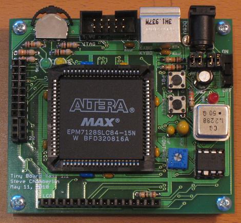
I built the board up in stages, with stage one being the power section, and stage two being the JTAG header and CPLD socket. After that, I was able to connect the board to my PC, and get the JTAG programming software to talk to it successfully. With that first checkpoint passed, I was confident the rest of the assembly would go fairly smoothly.
Once the assembly was finished, verifying the correct function of the buttons, navigation switch, and LEDs only took a few minutes. The LCD and keyboard interfaces proved to be more challenging, since I had to implement the behavior using basic Verilog logic instead of any kind of microcontroller or CPU. I had hoped to make a demo of reading keys from the keyboard and echoing them to the LCD, but unfortunately that wasn’t possible, because there’s no on-board memory in which to store the scan code conversion table. Instead, I made a demo in which the keyboard scan codes themselves are displayed on the LCD.
Without any kind of on-board RAM or ROM, I felt like I exhausted the possibilities of this board pretty quickly. A 128 macrocell CPLD without other support logic just doesn’t do anything very interesting. I guess that’s fine, though, since the whole point of this exercise was to get some PCB design practice, and get the experience of building a real board before moving on to the more complex board needed for the full Tiny CPU design.
I predicted I’d find four mistakes in the board design, but I only found two issues that I would call “mistakes”. Fortunately I was able to work around them both. Aside from those mistakes, I also found several other areas in which the design could be improved.
Mistakes
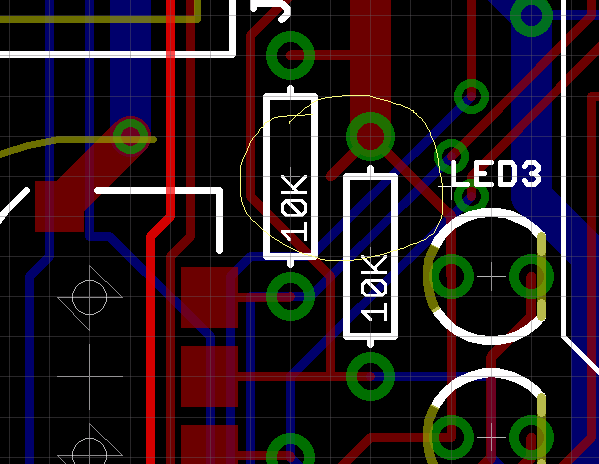
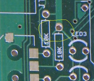
Reset circuit – The reset IC I’m using has separate output pins for the reset and /reset signals. Reset is a standard logic output, but /reset is open drain, and requires a pull-up resistor. I missed that little detail, and didn’t include a pull-up. To work-around the problem, I bent the /reset pin up and cut it off, then jumpered reset to /reset on the underside of the board, and changed the CPLD logic to expect an active-high reset signal instead of active low. You can see the cut-off pin at the bottom-right of the photo above. It’s pin 6 of the DIP-8.
PS/2 connector footprint – The PS/2 connector I bought had three through-hole “feet” for mechanical stabilization, in addition to the six signal pins. The footprint I used in Eagle only has one foot. My fix was to cut the other two feet off before mounting the connector on the board, which sacrifices some stability, but has no other negative effects.
Areas to Improve
Edge placement – The JTAG connector, PS/2 connector, and power connector all hang slightly off the edge of the board, which wasn’t intentional.
Component spacing – Components are packed in a little too tightly in a couple of places. All those little 0.1 uF capacitors surrounding the CPLD socket have to bend outward slightly, because they rub the socket’s outer wall. In retrospect, I should have left a little more breathing room between everything when doing the layout.
Expansion header power – The expansion header on the left side of the board doesn’t have any power or ground connections, limiting its usefulness. Instead, all the expansion pins are connected to CPLD I/O pins. Oops.
Test points – I didn’t include any test points or convenient places to connect an oscilloscope probe or signal tester. At least a spare pair of power and ground pins would have been handy.
JTAG connector – It would have been better if the JTAG connector were rotated 180 degrees. In the current orientation, the cable has to drape over the board, instead of off its edge. You can see this in the video.
Signal trace to nowhere – I must have forgotten to clean up an old trace completely while I was routing. During assembly, I noticed this signal trace that leads nowhere.
3 Comments so far
Leave a reply. For customer support issues, please use the Customer Support link instead of writing comments.
Even though you can’t do much with this board it does appear to be a successful test of design and construction, so good job on that!
I was just wondering if you prototyped any of this using separate components, breadboards etc. Or if you just went ahead and designed the PCB directly? I’m wanting to do something somewhat similar but I’m worried about making mistakes with both the circuit and the board layout.
If so, then I’m pretty impressed it worked with few problems to be fixed 🙂
I guess I should probably get a board made up for one of my microcontroller projects that I’ve made on a breadboard first then at least I know the basic design is right, and it will also give me some practice at constuction.
I did some prototyping experiments with the same type of CPLD and a commercial wire-wrap board, but it was pretty different than what went on the PCB. So yes, I was also surprised that it worked with few problems!
Making a simple test PCB for a microcontroller project sounds like a great way to start. Really, the prices on small custom PCBs are low enough now that I wouldn’t feel too bad about screwing up a couple until you get the design right.