

JTAG, EXTEST, and hair loss
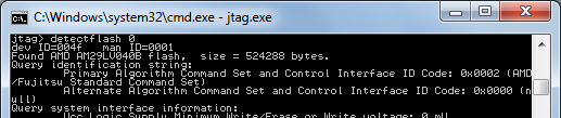 Oof. See that window to the left? That’s the result of 10 hours of debugging effort on bring-up for my custom Tiny CPU board. What you see is UrJTAG connected to the JTAG interface of the Max II CPLD, and successfully detecting the 29LV040B flash ROM that’s also on the board. Getting to this point was a long process covering everything from software to cleaning up bad solder joints.
The good news: I’ve soldered the Max II CPLD, Flash ROM, and SRAM to the board, and they seem to be working. By using UrJTAG and the EXTEST instruction, it’s possible to disconnect the CPLD’s core logic from the pins, and set the pin states to any arbitrary values. The software also needs to be told which pins are connected to the address bus, data bus, CS, OE, and WE. Once that’s done, it’s possible to read and write any non-JTAG device whose pins are connected to the CPLD, by bit-twiddling the CPLD pins. Using UrJTAG’s commands for memory access, I’ve successfully written and read from the on-board SRAM, and reprogrammed the on-board Flash ROM. That should be nearly everything that’s needed to start work on the Tiny CPU core itself.
Interaction with the Programmed Design
I find JTAG and especially the UrJTAG tool to be maddeningly difficult to understand. Things don’t work how I’d expect, or don’t work at all, and I can’t be certain if it’s a hardware problem, software bug, or misunderstanding on my part. The best example is the reason that it took me so long to reach the point where the Flash ROM was successfully detected: interaction between the core logic (the design programmed into the CPLD) and the EXTEST pin manipulation. From what I’ve read, there should be no interaction. When the EXTEST instruction is executed by the JTAG controller, then the pins should be decoupled from the core logic. It shouldn’t matter at all what design is programmed into the CPLD, what that design wants to do with the pins, or whether any design is programmed at all.
After long experimentation and electrical testing, I discovered that the core logic design does matter when interfacing to other devices with EXTEST. Whether this is normal, or the result of a boundary scan software bug in UrJTAG, I don’t know. What I found is that if I programmed the CPLD with a design that declared the data bus as type inout (which it is, of course), then I could read from the SRAM and Flash but not write to them. By sticking a multimeter on the pins, I found that data bus pins driven to a logical 0 using EXTEST worked fine, but data bus pins driven to a logical 1 just went into a high-Z state instead, so I could never write a ‘1’ bit. I also learned that if I set the data bus type as output, then I could no longer read from the RAM or Flash. Only when I set the data bus type to input could I both read and write using EXTEST. This is nonsense on a several levels, as it shouldn’t be necessary to reprogram the CPLD with a new design just to use the EXTEST functionality. The only explanation I can think of is that the boundary scan register uses 3 bits to define the state of each pin (input, input with pull-up, output driving 0, output driving 1, output driving Z, and a few others) which UrJTAG may not handle properly, with some bits carrying over from the programmed design. I had a similar problem when using a trial version of TopJTAG Flash Programmer, however, so I’m not sure I can blame the software.
JTAG Bit-Banging
As another example of UrJTAG strangeness, the board has an LED connected to IO97, such that the LED illuminates when the pin value is 0. It should be possible to blink the LED using UrJTAG’s set signal command, e.g:
jtag> set signal IO97 out 0
After much tearing out of my hair, I learned that while that’s part of it, it’s also necessary to explicitly put the device in EXTEST instruction mode first, and explicitly shift the instruction and data into the device, as UrJTAG does none of this for you:
jtag> instruction EXTEST
jtag> shift ir
jtag> set signal IO97 out 0
jtag> shift dr   (the LED turns on)
A little cumbersome, but at least it works. In contrast, I was never able to get the corresponding get signal command to work at all. After setting IO97 to 0 as above, which visibly turns on the LED, the value of IO97 still reads as 1:
jtag> get signal IO97
IO97 = 1
jtag> shift dr
jtag> get signal IO97
IO97 = 1
The ability to twiddle pins arbitrarily through JTAG could be a huge aid to debugging, but not if the corresponding ability to read the current pin state doesn’t work.
If anyone has some experience using UrJTAG for this kind of troubleshooting, please leave a comment, or contact me by email. Thanks!
Read 5 comments and join the conversation5 Comments so far
Leave a reply. For customer support issues, please use the Customer Support link instead of writing comments.
Ah, things make more sense now. My inability to use “get signal” for the LED or to read ROM/RAM when the databus type is set to output is explained by this paragraph from the Max II datasheet:
The interaction between the programmed CPLD design and EXTEST outputs also appears to be something similar. While I can’t find documentation that confirms this, it seems that if a pin of type inout doesn’t have any driver defined in the design (which my test design didn’t), the Quartus II software will conclude that the pin’s output enable circuitry is unnecessary and disable it. I confirmed that as long some logic somewhere in the design can drive that inout pin, even if it’s never exercised, then EXTEST outputs on that pin work as expected.
So if I understand correctly, you are trying to use the jtag interface (urjtag software) to toggle or read I/Os on the device that hangs off the cpld? For those GUI inclined, something like this : http://www.topjtag.com/probe/ ?
If so, I’ve always thought the openOcd project can do all that urjtag can do, but is a bit more mature and perhaps more user friendly. Have you looked into OpenOCD?
A lot of inexpensive jtag programmers have the ftdi chipset, which urjtag and openocd both support, so is there an advantage with urjtag?
urjtag is largely designed by and for fpga coders. Likewise OpenOCD for micro guys (especially ARM). There is alot in common, but I haven’t seen working get/set or svf functionality in the versions of openocd I’ve tried. Plus it’s a royal pita to configure, whereas urjtag is pretty much plug & play once you’ve figured out your dongle settings and bsdl file. OpenOCD is more of a script language you need to learn in my mind.
Thanks for this post, by the way! You are the only resource on the web who has apparently read the source to urjtag to figure out set (it sure ain’t in the examples/manual/website). Get worked right out of the box on my Xilinx fpga, fyi.
Thanks!!
Thanks to this post I could get to change the pin output on a Cyclone III FPGA, using USB-Blaster and UrJTAG.
I could only read up until now. I was missing “instruction EXTEST”
Bye!!
hello!
how it’s done — “The software also needs to be told which pins are connected to the address bus, data bus, CS, OE, and WE”?
You’ve modified some config file of urjtag or something? just can’t find info how to do this(