

Invalid Logic Levels Explained
What happens when you feed an invalid voltage level to the input of a digital logic gate? It’s an interesting story. In my last post, I described a subtle Nibbler bug where a combinatorial feedback loop through the ALU caused an invalid voltage level to propagate from an output back to the input, creating a self-sustaining cycle of badness. I fixed the problem by adding another chip to break the loop, but I wasn’t totally happy with that solution. After studying the problem further, and peering into the internal details of the 74LS181 ALU chip, I’ve found a new solution that doesn’t require any extra hardware. The new chip has been removed, and Nibbler still runs flawlessly.
To explain what’s going on, it’s important to understand how basic logic gates like NOR and AND are built from transistors. The diagrams below show gates using FET transistors, instead of the bipolar transistors used in the 7400LS family, but the concept is the same.
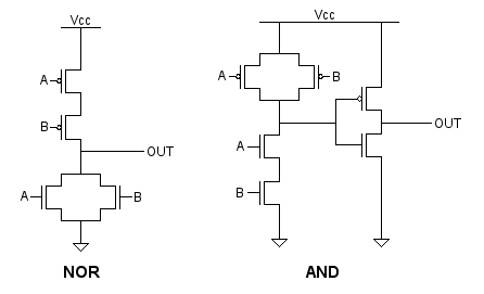
In the NOR gate, if either A or B is above the transistor switching threshold, one or both of the bottom transistors will be turned on. This pulls the output to ground. The top transistors will be turned off. If neither A nor B is above the switching threshold, neither of the bottom transistors will be turned on, but both of the top transistors will be on, pulling the output to Vcc.
In the AND gate, the top and bottom portions are reversed, and an inverter is placed at the output of the first stage to create an AND instead of a NAND.
Now let’s assume B is at an invalid voltage level, right around the transistor switching threshold, while A is zero volts. In the NOR gate, one of the bottom transistors will be off, and the other will midway between off and on, acting similar to a resistor. One of the top transistors will be fully on, and the other will be midway between off and on. The result is that both the top and bottom sections will be partly on, creating a path from Vcc to ground, and resulting in an output voltage that’s somewhere in the middle.
If B was invalid while A was at Vcc, then one of the bottom transistors would be fully on, and it wouldn’t matter that the other bottom transistor was midway between off and on. Similarly, one of the top transistors would be fully off, so the other transistor wouldn’t matter. The output would be 0 volts regardless of the voltage at B.
Applying the same reasoning to the AND gate, these rules emerge:
- ? NOR 0 = ?
- ? NOR 1 = 0
- ? AND 0 = 0
- ? AND 1 = ?
Now let’s apply these rules to a section of the 74LS181 internal logic, taken from its datasheet. In the case where Nibbler was failing, the ALU function input S was all 1’s, the A input was also all 1’s, and the B input was momentarily at an invalid voltage level. The blue numbers show the propagation of values through the first input stage of the ALU.

In this case where S is all 1’s, the ALU output is supposed to be A, and the B input shouldn’t matter. And logically, that’s what happens. The three gates on the right compute the expression A0*/B0*S2 NOR A0*B0*S3, which here reduces to /B0 NOR B0, which is always 0 regardless of the value of B0. So B is irrelevant. But electrically it’s a different story. The ? values propagate through the gates. ? NOR ? is not 0. The ALU outputs ? values to the data bus, which eventually propagate back to its B input, continuing the vicious cycle. The circuit doesn’t work.
But wait! On the ‘181 ALU, there are actually two different ways to output the value of A. I arbitrarily chose one of them when I designed the microcode. The other way sets the ALU function input S to all 0’s instead of all 1’s. What happens in that case?

The ? values are stopped dead at the first input stage, and don’t propagate any further into the ALU. The circuit works.
Applying this to Nibbler was easy. I just changed the microcode to use the 0000 output function instead of the 1111 function, and removed the extra chip that I previously added to break the feedback loop. Happy times!
Read 2 comments and join the conversation2 Comments so far
Leave a reply. For customer support issues, please use the Customer Support link instead of writing comments.
Otherwise, if you keep the mux and connect the A-reg to its input right shifted one step, then you have prepared for a shift right instruction. Connect carry to bit3 and some thinking in micro-ROM, you have both LSRA and RORA.
Sorry just a little brain-run-away, time to go to bed now…
I\’m pretty sure a nearly identical feedback problem is lurking in my Gigatron TTL computer. The reason it doesn\’t cause havoc is not as clear. The feedback goes to the multiplexers in the ALU (same as here), and those are looking at the other input when this occurs (same as here). But from the logic diagram alone you can\’t say if an input glitch will propagate or not. Actually, in the Gigatron case the logic diagram predicts that there WILL be glitch that causes some instructions to malfunction. I think we just got lucky for some even more obscure reasons. https://github.com/kervinck/gigatron-rom/issues/78