

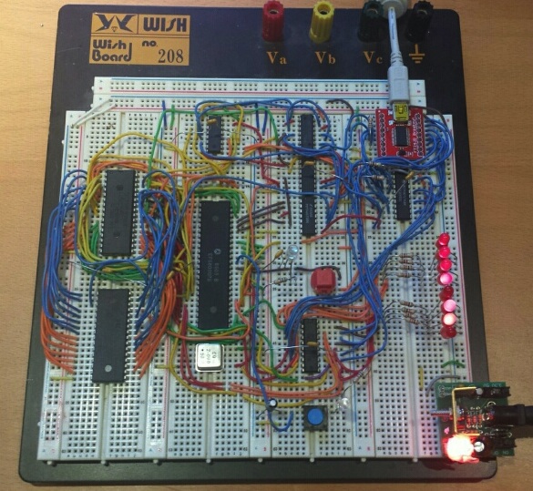
Breadboarding the 68K
My 68K breadboard computer is alive! It’s always a thrill when a pile of random chips does something recognizably computer-ish for the first time. Blinking some LEDs in sequence is great; running BASIC is super extra great. I’m excited.
This simple breadboard machine is a prototype of the 68000 single board computer I plan to build next. By testing the key design ideas in a breadboard prototype, I hope to uncover any lurking design problems while they’re still easy to find and fix. Once the design is committed to a PCB with lots of tiny surface-mount components, it will be much more difficult to make changes. Even probing specific signals to observe what’s happening may be difficult. The breadboard is a much more forgiving place to experiment and learn.
Compared to my plans for the final 68000 machine, this breadboard version has less memory, a lower clock speed, a narrower data bus, fewer peripherals, no interrupts, and glue logic built from discrete chips instead of a CPLD or FPGA. Except for the serial interface, the whole thing was built entirely from parts I had on hand. The specs are:
- 68008 CPU running at 2 MHz
- 256K Flash ROM
- 512K SRAM
- USB to parallel serial port
- 8 addressable LEDs for debugging
- Miscellaneous 74LS and 74HCT chips for address decoding and glue logic
The computer doesn’t use interrupts – it always runs at the highest interrupt level, and polls the serial port when it needs input. It also doesn’t use any of the CPU’s DMA or legacy 6800 peripheral support. There’s no handshaking for memory accesses either. The /DTACK signal that devices are supposed to use to indicate a successful memory transfer is just hard-wired to ground – the so-called DTACK Grounded approach to system design.
The Build
Getting the machine up and running went surprisingly smoothly, and only took six days of occasional work. The biggest challenges were the hidden 250 mA PTC fuse in my power supply, and noise in the /RESET signal. Other than that, it was just a matter of placing all the chips on the breadboard and stringing a few hundred wires to connect them.
It was tedious work to perform all the address decoding with discrete logic instead of a CPLD. It’s so nice to type a Verilog equation like /CS = A19 * A18 * /AS * (/F0 + /F1 + /F2), and so annoying to wire up the equivalent equation from a bunch of individual AND, OR, and NAND gates. I quickly ran out of gates, and wasn’t able to decode the address space as fully as I’d hoped, or cover all the reset-related edge cases. It gave me new respect for how useful even a tiny CPLD can be for consolidating glue logic.
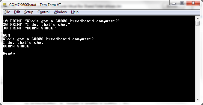
The first test programs were written using the Easy 68K editor and assembler. It was a huge help to run the programs in the Easy 68K simulator, to make sure they worked as intended before trying them on my hardware. There’s nothing worse than staring at a non-functional DIY computer with no way to tell if you’ve got a software bug or a hardware one.
Easy 68K assembles programs into Motorola S-record files, which I opened with my EPROM burner software, and programmed into my Flash ROM. That was all I needed to get some basic LED blinker programs going. Physically moving the Flash ROM chip back and forth between the breadboard and the EPROM burner wasn’t much fun, though, so I wrote a quick and dirty bootloader. The bootloader is stored in ROM, and runs when the computer is first turned on, waiting for data to appear at the serial port. The first four incoming bytes define the size of the transfer, then the remaining data bytes are stored sequentially starting at the RAM base address. After the last byte is transferred, the bootloader jumps to the RAM base address to execute the program that was loaded. It’s not fancy – there’s no acknowledgement, or checksums, or facility for alternate load or start addresses. But it’s enough to experiment with new programs without having to unplug the ROM chip each time.
Once I had a working bootloader, I started searching for 68000 software that could be easily ported to this hardware. Lee Davison’s Enhanced Basic for 68000 is well known for being excellent in this respect. All that’s needed is to change a few assembler definitions for RAM base address and size, and to provide implementations for the routines to get or print a character. The rest is just vanilla 68000 assembly code with no platform dependencies. Unfortunately it appears that Lee Davison passed away recently, and his web site is gone. I wasn’t able to find an original version of Enhanced Basic anywhere. In the end, I used an Easy 68K specific version of Enhanced Basic, then ripped out all the Easy 68K specific parts. It took me a while to discover some Easy 68K specific modifications that had been made to the “platform independent” part of the code (naughty, naughty), but it still only took a few hours to get Enhanced Basic up and running on the breadboard hardware.
Next Steps
With 512K of RAM, it might be possible to bootload and run a super-minimal version of ucLinux. Even if it’s not possible, I expect I can learn a lot from the attempt. So I’ll be downloading the ucLinux source and getting familiar with how to build it and modify it. That should keep me busy for a while. 🙂
On the hardware front, I found one potential problem that I’m unsure how to handle. During the first half clock of every bus cycle, the 68K CPU puts its address and data lines into a hi-Z state. And during reset, the CPU puts virtually all of its outputs into a hi-Z state, including the address strobe and other control signals. This is a big problem for my address decoder and other glue logic, because they basically blow up if their inputs aren’t well-defined 0’s and 1’s. At best their outputs will be wrong or at invalid voltage levels. At worst they’ll consume a ton of current or enter some crazy oscillation, injecting noise everywhere in the circuit. I’m not sure why my breadboard prototype doesn’t exhibit problems like this already, but I suspect I’m just lucky. The full-scale 68000 system on a PCB may not be so lucky.
What’s the best way to fix this problem? Other homebrew 68K designs I’ve looked at don’t mention it. I could put a weak pull-up resistor on every CPU output, to gently pull it to a valid voltage level if the CPU isn’t driving it. But that would be a lot of resistors, and it might increase the signal rise/fall times during normal CPU operation, reducing the maximum clock speed that can be reached. Hmmm.
What’s In A Name?
This 68K effort needs a name. My other projects all have vaguely humorous names or name puns: Big Mess o’ Wires, Nibbler (the 4-bit CPU), Plus Too, Floppy Emu, etc. For this project I’m thinking of 68 Kangaroo, keeping with Floppy Emu’s Australian wildlife theme and extending 68K with an -angaroo. Other ideas along the same line of thinking are 68 Katy (my wife might be jealous), or 68 Kale (try it sautéed with garlic). Single Bored Computer also has a nice sound to it, and would be great for online dating. Ah, the possibilities…
Read 18 comments and join the conversation18 Comments so far
Leave a reply. For customer support issues, please use the Customer Support link instead of writing comments.
Wow, you work fast! I love the breadboard picture.
Resistor packs can be convenient for bus pull-down or pull-up resistors, especially the kind that comes in a SIP or DIP with one side of all the resistors tied to a single pin.
Also, TI makes logic parts with a “bus hold” feature that keeps a bus at its last state until it is driven to a new state. There are specialized parts that do only this and regular functions that happen to have it on their inputs. Search for “Texas Instruments bus hold” and you will get a bunch of relevant links.
Stephen
Oh dear, very sorry to hear about Lee Davison. RIP. I do hope somebody has an archive of his 6502 and 68000 BASICs somewhere.
You mentioned using a CPLD or FPGA for the eventual board layout. I am a hobby computer fan, and also an FAE for Lattice Semiconductor (disclosure, didn’t want to be seen as selling parts). Most of the newer programmable logic parts have options for pullup or bus hold built into the I/O buffers. The bus hold is intended to counter just the problem you mention. They will lightly hold the last driven value on a bus, can be easily over-ridden when the next value change happens, and do not require any external parts (resistors) on the PCB. So this would get you the bus hold feature right along with your logic decode, all in one chip. Glad to pass along more info if interested. Good luck with the next steps in your project.
Ken
Thanks Ken. Is that only for the CPLD pins configured as outputs, or does bus hold work for inputs as well? I would also be interested to know what JTAG programmer I’d need to get started with Lattice parts – is there a proprietary one, or will some generic one work? I’ve noticed Lattice often has similar programmable devices to Xilinx/Altera at lower prices, but wasn’t sure how to start experimenting with them.
I thought about this a bit more after my last comment. The biggest issue I think will be that you probably need 5V logic, and there are almost no 5V programmable parts left. Lattice has one family that is 5V tolerant, and operates on a 3.3V supply (LC4000 family). The pullups, or bus hold would work for either ins or outs. The official programmer for Lattice is around $150, but there are various third part options. If you buy one of the eval boards (around $30) they have programming built in for the part on the board, and with a little cut and jumper work, can be connected to program any board.
For the final board I plan to use the 68ec000, running at 3.3v.
I’ve got a copy of the source for ehbasic v3.49 for the 68k. Send me an email if you’d like a copy
Hint: use 74LS/74HCT multiplexers for address decoding instead of discrete logic gate. It is then straightforward to convert your logic equations into wiring and much easier to modify:
http://6502.org/users/dieter/a1/a1_4.htm
It will also provide much more consistent timings than an uncontrolled-depth cascade of logic gates.
@Michel Stempin – You’re right, and I glossed over some details in the write-up. I’m using a 74LS139 decoder for the actual address bits A16-A19, but there are other signals also needed for address decoding (AS, DS, F, RW) that are using those AND/OR/NAND gates.
Although the spec says unused inputs should be tied hi or low, LS inputs have sort of an internal pull up and almost all ways float hi. So its not surprising the ls139 works fine. CMOS inputs left floating are way more prone to oscillation and may draw high current.
A PLD like a 22v10 might be a better choice than a CPLD. They are cheap, available in DIP, and run @5v.
On naming: just as resistor values are sometimes represented as 2k2 for 2200 ohms, how about 6k8, or perhaps 6Kate, which is close to your 68 Katy?
On bus pull-ups: the Mac 512k schematic I have shows a 2k2 SIP pull-up on A[1:12] and A19. The data lines are driven by LS244 tri-state buffers.
Ok on using 3.3V part, that makes finding current logic devices so much easier. You could use the LC4000V family; which is 3.3V core with two I/O banks. Easier to use than 22V10 and probably cheaper. Or, you could go to an LCMXO2-256HC or LCMXO2-640HC in a 100TQFP and have lots of logic, and I/O along with built in I2C and SPI interfaces. These are instant on parts that run on one 3.3V supply. There is a third party offering code to program the XO2 part via SPI using a Raspberry Pi board. So cost and simplicity vs. flexibility kind of trade off. Simple breakout boards available for either family to try things out for low cost. Development tools are free download with free license. Hope that gives you options to think about.
Ken
First off – bravo for getting this off the ground & running. Amazing stuff.
I worked for Mostek (way back, early 80’s), and I built a M68000 In-Circuit Emulator for developers. It was a major cost-cutter, since the Motorola Emulator cost around $36000 at the time and didn’t have the features we had (and it was buggy). Mostek was a 2nd source for the 68k. Sadly, Mostek failed in the memory IC business before we could sell very many.
The emulator consisted of a pod with a 68k in it, controlled by a bigger box with a Z80 which controlled it, setup breakpoints, disassembled 68k. It was a memorable project.
I can tell you, that in the lab – PC and Wire-wrapped boards, not Breadboards – we were able to run it successfully down to about 50 hz clock. It’s a very sturdy CPU with a really nice instruction set.
Very cool, sir. Well done.
Mike Yancey
Dallas, Texas
I too like Jeff’s naming idea. I personally think it should be spelled 6K8, but pronounced 6Kate.
A MachXO2 would be great. One could implement some MMU too 🙂
Ca the 68k run down to 50 Hz ?, Ok, one should not take everything what the manual says as the absolute truth but they mention 2 MHz as the minimum clock… I thought it had dynamic ram cells for the registers…
Excellent job! I love seeing the oldies-but-goodies fired back up doing something interesting.
I’ve got a special place in my heart for BASIC, as it was, for better or for worse, my first programming language.
I stumbled across this page and was amazed to see that the 68K is still available. I began my professional career getting an early RTOS to run on a custom 68000 board my then-company was building back in the early 80s to control a bunch of signal processing equipment. The C language was just coming in vogue and we used an early version of a C compiler to build our application code for the CPU.
New CPU + new OS + new compilers = tons o’ fun!
Great article. Brings back some good memories.
I worked years with a 68008. For the Hi-Z outputs between memory cycles that is intentional. It allowed other bus masters to suspend the 008 and take over the bus for a while, like for DMA. For single processor simple systems not needed. Pull those A & D lines up and everything else you don’t need/want, use a resistance that does not exceed the 008 rated Iol with your other bus loads. The smaller the resistance the faster the pullup (RC time constant). The Hi-Z to low transition should not be to affected much by the resistor value as long as you don’t overdrive the IC output gate.
In any event the 008 is robust so just try out some ideas. I don’t think I ever killed one due to a design experiment or error.
The 008 can run at 8MHz and getting a dtack circuit to match your RAM access time should not be too difficult to design.
But for more fun grab onto a 68332 which runs at 24MHz, has Dtack generators, better addressing modes and is even more pleasant to work with. Innovasic makes a chip that is intreresting, a COPU32 with 66MHz and lots of I/O built in.
IMO Mot/Freescale screwed up by coming out with the Coldfire and making no EASY forward going alternative. Not that they aren’t fast and all that but you can’t just make a few tweaks and have you 68K / CPU32 code work. Sigh.