

Daisy Chain Adapter Progress
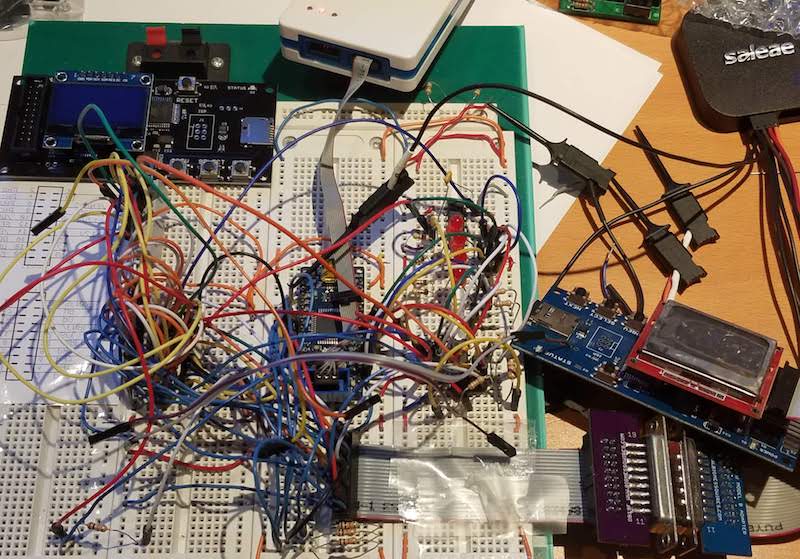
I’m still working away on the daisy chain adapter concept for Floppy Emu, and I’ve prototyped something that mostly works. It’s a real mess on the breadboard. There’s an AVR microcontroller in there somewhere, plus some open drain buffers, some NAND gates… I think I also saw an engine controller from a 2003 Ford Focus. Yikes. I solved the pulldown problem described in my previous post by incorporating the proposed SR latch circuit.
For readers who may have forgotten, the goal of this project is to design a Floppy Emu accessory that:
- adds a daisy-chain output port, to attach more drives
- addresses some existing Floppy Emu daisy-chain limitations
- possibly includes a signal debugging interface or other goodies
It’s imagined as a T adapter. Power and input signals will come from the computer or the upstream drive in the daisy chain. One branch of the T will connect to a Floppy Emu. The other branch will connect to a real disk drive, or multiple drives in a chain. From a logical perspective, these drives will appear downstream from the Floppy Emu. This will enable the use of complex multi-drive setups involving a Floppy Emu and other drives that may not be possible otherwise.
After looking at this concept from every angle, I’ve concluded it will need these elements:
- combinatorial logic – roughly 8 inputs and 8 outputs
- three or four bits of state, ideally implemented as SR latches
- open drain buffers
- power-on reset circuitry
- maybe a clock source
- assorted levels shifters, pull-up resistors, etc
- a DB-19 male and a DB-19 female
My leading plan is to use a simple AVR microcontroller as the heart of the device. But since that’s far from an obvious choice, let’s take a look at some alternatives.
Discrete logic – I could build the whole thing from common 7400-series parts like NAND and NOR gates, with a few extras for things like power-on reset. But the part count and total cost would be higher than the alternatives. It would also prevent me from experimenting with different logic equations and different behaviors.
Parallel ROM – An 8 input, 8 output logic equation can be implemented as a 256 byte ROM. It’s reprogrammable. But the ROM wouldn’t help with the other needed elements, and in-circuit reprogramming of a parallel ROM is annoying. 5V ROMs are also increasingly rare and more expensive than the alternatives.
CPLD – This was my original plan, and is still a possibility. Any combinatorial logic can be easily programmed or changed in a CPLD. But there are headaches. CPLDs don’t like to make latches. Without latches, I need a clock source, which some otherwise-promising CPLD types lack. Most CPLDs are also 3.3V or 1.8V, requiring 5V level shifters on both the inputs and outputs.
AVR – Even the simplest AVR microcontroller can run at 5V, has a built-in clock, has a power-on reset circuit, and has built-in pull-up resistors. They’re extremely flexible for debugging or experimentation. And they’re cheap: for the cost of two or three 74LS00 chips, I can have a full-blown microcontroller. The combinatorial logic can be implemented in code. Read the inputs, do a table lookup for the logic function, set the outputs, repeat.
Logic Delays
The one big drawback of an AVR solution is that the combinatorial logic function will be much slower than the alternatives. Even with a tight code loop, the delay from input to output will be 1 or 2 microseconds, compared to 10 to 100 nanoseconds for the other alternatives. This delay will put the processed disk control signals slightly out of phase with the other disk signals. (Yes I know there are some microcontrollers with built-in programmable logic, but I’m not going there.)
Beyond some level, the combinatorial logic delay will cause disk errors. So how fast does it need to be? The short answer is 1) it depends, and 2) I don’t know.
It depends, because some signals appear more sensitive to delay than others. From my limited tests, the PHI3 signal is much more sensitive than the /DRIVE1 and /DRIVE2 enable signals. So one option is to partially handle PHI3 with hardware gates, and do the rest in software.
The exact level of tolerable delay is something I’ll need to test, and I’m not sure where the worst-case scenario lies. A PHI3 delay of 3.5 microseconds prevented a 3.5 inch drive from working, but 2.5 microseconds seemed OK. /DRIVE1 and /DRIVE2 appeared able to tolerate delays up to 20 microseconds. But I don’t completely trust those numbers yet.
So what now? I’m attracted to the AVR solution, and I think there’s a good chance it’ll work, but I won’t really know until I design and build a PCB and test it thoroughly. There are too many problems with signal integrity and grounding in my breadboard circuit to fully trust it. I’m undecided how to handle PHI3. Maybe I’ll design a PCB that can either handle PHI3 in software or in hardware gates, and try both ways. Then I’ll need to design a second, final version of the PCB once I’ve found the timing limits. Onward!
Read 2 comments and join the conversation2 Comments so far
Leave a reply. For customer support issues, please use the Customer Support link instead of writing comments.
Makin’ progress. Seems promising.
Thanks, after testing it seems to mostly work. With a Floppy Emu and a 2nd Floppy Emu as the daisy-chained drive, it works for all the valid combinations of drive types. But when I connect a real drive as the daisy-chained drive, things often go bad when the real drive’s motor turns on, and especially when a 5.25 inch drive makes that signature click-click-click noise. I think the drive motor is pulling a lot of current from the +12 and -12V supplies, and even though Floppy Emu doesn’t use those, it causes trouble. The Emu frequently resets or just goes dark. Probably due to the poor breadboard wiring…