

Yellowstone 2.0 Layout and Route
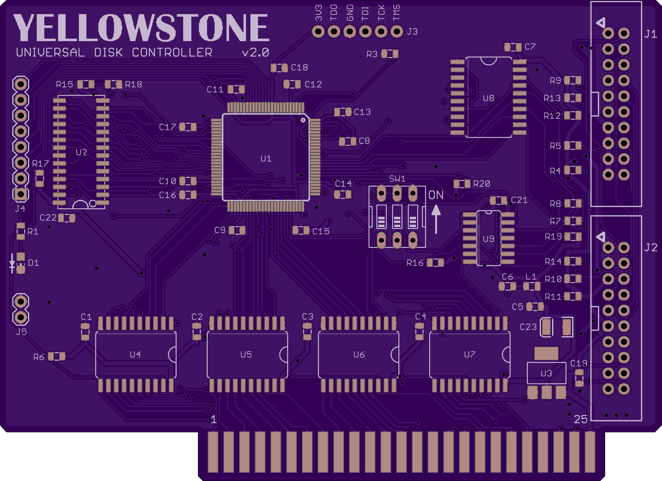
It took longer than expected, but the PCB layout is finished for version 2.0 of the Yellowstone disk controller. Phew! There’s still a bit of cleanup work to be done before I send the board for manufacturing. Hopefully I can finish that off within the next few days. I think it’s getting close.
Quite a lot has changed from version 1.0. The board now has two disk ports instead of one, with some DIP switches to control how they’re used. A 32KB RAM is now paired with the FPGA, reducing the amount of internal block RAM that’s needed and hopefully (to be confirmed) enabling me to use a lower-end member of the FPGA family that’s cheaper and more widely available. Level shifters and open drain buffers are now present on all of the disk I/O signals. In normal use none of the FPGA’s pins will be directly connected to anything off-board, which should improve robustness. The 3.3V regulator is now rated for 800 mA instead of 300 mA. I’m not convinced this was really necessary, but it’s something many people suggested upgrading from the 1.0 design. All of the chips except the FPGA are now using SOIC packages with 1.27 mm pin spacing, to make soldering easier and reduce the chances of assembly problems. Version 1.0 mostly used TSOP packages with a much finer 0.55 mm pin spacing.
Too bad there are no 5V FPGAs anymore. Half the chips here are dedicated to level shifting, and could disappear if the FPGA used the same voltage as the disks and computer.
The board routing is improved too, although you can’t tell from looking at the image. The edge connector on Apple II peripheral cards only has one pin for each power supply voltage, including ground, so it’s important to make those PCB traces nice and wide and to minimize the number of vias between the supply and the load. Yellowstone version 1.0 did a poor job of this.
I added a very simple bus sense input that could be used to support batch testing. It’s just a voltage divider connected to the 12V supply. If the FPGA sees this input high, it can assume the card is installed in an Apple II. If it’s low, it can assume it’s on a test bench and alter its behavior accordingly. I’ll figure out the rest later.
I can’t resist looking into the future and observing that chips U1 through U7 could be used as-is for many purposes other than disk control. Those chips form a generic design of an FPGA plus 32K RAM with level shifters connected to the Apple II bus. Only chips U8 and U9 are really specific to being a disk controller, because they determine the direction and I/O voltage of the signals on the disk ports.
Parts availability may be a problem here. Most readers have probably heard about the global IC shortage that’s affecting everybody right now, and BMOW is no exception. The prices of many ICs have increased significantly, and some types of ICs have become difficult or impossible to find anywhere.
A question for PCB designers and assemblers: when a board like this one has dozens of passive components, how do you decide on a numbering scheme? Is it better to number them in order according to their physical location on the board, making them easier to locate quickly? So for example the column of resistors on the right could be numbered consecutively R1 through R11. Or is it better to number them so that components with the same values/types have consecutive numbers, regardless of where they are on the board? So for example R1 through R6 might be all the 10K resistors, then R7-R10 could be all the 6.8K resistors, and so on.
Read 9 comments and join the conversation9 Comments so far
Leave a reply. For customer support issues, please use the Customer Support link instead of writing comments.
Parts are usually numbered by their place in the schematic. Most tools offer a way to do that automatically.
I’d recommend routing the power supply tracks first to the decoupling cap and then to the IC pin to improve its effectiveness. Also you could add via to the bottom ground plane next to each cap’s ground terminal. I think you might even get away with removing ground on the top layer completely, as the bottom plane should not be disrupted by many tracks.
For prototype assembly and debugging I find the InteractiveHtmlBom tool extremely helpful.
Stupid question: Have you considered using a GAL paired with an MCU as a 5v tolerant a replacement for an FPGA?
I usually renumber the parts after PCB layout is complete so they’re (more or less) in order by location. It helps finding them on the board.
The machine doing the assembly doesn’t care at all. It’s just the person debugging / repairing it who does.
@Alex Cat3
The MCU has a non-zero startup time, especially when using a fast ARM-based one that has to get its PLL up and running before being useful. That conflicts with the fast responses required by the Apple (see for example https://www.bigmessowires.com/2021/04/22/floppy-emu-update-smartport-daisy-chain-support/).
The FPGA is ready as soon as power is connected.
I was surprised to learn that the FPGA actually takes some time to load its configuration data from internal flash to internal SRAM before it enters user mode and is ready to go. The datasheet didn’t quantify this time exactly, but says it’s “milliseconds”.
Convention I’ve almost always seen if numbered according to schematic location. Generally these partz are physically close to one another anyway.
Revisions can introduce exception of course.
Maybe it’s a good idea to provide a layout option for a version using a 32-pin 628128 128 kB SRAM instead of the 32 kB SRAM? This would enable the implementation of accelerators using a CPU soft core in the FPGA with a more useful amount of on-card SRAM.
That’s an interesting thought. It would take more than just extra RAM to make an accelerator though. The address bus would also need to be bidirectional, and all 16 address lines would be needed (Yellowstone only uses 12 or 14). And I think it would also need the DMA signal? I’m not sure how accelerator cards normally pause the host CPU and force it to release the address and data buses.
I think the current hardware is better suited to acting as a peripheral. It’s intended as a disk controller, but it should be fairly easy to make it behave as a parallel or serial interface card with just a wiring adapter. It could probably also function as a basic video card. Maybe also an Ethernet adapter, but I think that would be much more complicated. Possibly also as a USB keyboard adapter, though I’m not sure how it would hook into the normal keyboard routine. I have some other more ambitious ideas that I’ll share later.
Bidirectional address lines shouldn’t be that problematic. I don’t know which level shifters you use in the current design, but the GODIL FPGA modules use TI’s 74CB3T16211 bidirectional level shifters, which have 24 lines (details at https://www.trenz-electronic.de/trenzdownloads/OHO-Elektronik/TE0261-GODIL/archive/UM_GODIL-v090.pdf). However, I don’t think the TI ICs come in a convenient 1.27mm package.
I think taking over the bus works via asserting /DMA (and releasing it from time to time so the 6502 doesn’t lose its register contents), but I never designed a bus master card. Some interesting information can probably be found at https://retrocomputing.stackexchange.com/questions/8087/how-do-accelerators-and-cpu-cards-work-on-the-apple-ii and https://www.applefritter.com/appleii-box/harrowalsh.de/Elektronik/APPLEBOX/68008CPUcard/68008translation.pdf
But I agree, the overhead to convert the design to be able to implement bus master access might be too high.
But even without support for bus master operation, increased RAM size might still help to build an ethernet card – some interesting alternative designs might be clones of the SuperSerial card or a LocalTalk adapter?