

First Look at the RP2040 – Raspberry Pi Microcontroller
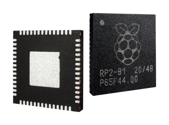
In response to my last post, a few readers suggested looking at the Raspberry Pi Foundation’s RP2040 microcontroller for possible use in a future Floppy Emu hardware refresh. The RP2040 was announced in January 2021, first as part of the Raspberry Pi Pico development board, and later as a stand-alone chip. While Raspberry Pi’s other offerings are essentially full-fledged computers, the RP2040 is a traditional microcontroller that will compete directly with familiar products from Microchip, ST, Espressif, and NXP. So what does it offer that might set it apart from the competition? Is it worth a look? Here’s my take.
Strong Points
RP2040 is a 133 MHz dual-core ARM Cortex M0+ microcontroller, with 264 KB of RAM, and a unit price of $1 USD. Right off the bat, that looks appealing. I don’t know of any other microcontroller from a major vendor that offer a better ratio of hardware specs per dollar. 133 MHz is quite zippy, and 264 KB of RAM is substantially more than any of the alternative parts I’ve been considering. Dual core is just icing on the cake.
The hardware also includes two programmable I/O (PIO) blocks with interesting potential. These are hard to describe in a single paragraph, but they’re like high-speed specialized coprocessors that could replace much of the software-based bit-banging that’s often needed in microcontroller applications. They’re a good fit for high-speed bit twiddling, independent of the main cores. For the Floppy Emu, PIO blocks could probably be used to replace some of the specialized logic that’s currently handled by a CPLD programmable logic chip.
The documentation looks well-written. So far I’ve reviewed the chip datasheet, hardware design guide, the C/C++ SDK documentation, and the Getting Started Guide.
The RP2040 is available and shipping in large quantities right now, which is quite an accomplishment given the current shortages everywhere else in the industry. DigiKey has over 50000 in stock. You can also order the chips directly from Raspberry Pi.
Weak Points
There’s zero flash or non-volatile memory for program storage on the RP2040. All the application code and data must be stored in an external flash chip. Six dedicated pins are used to communicate with a separate QSPI flash, using execute-in-place (XIP) technology to run code directly from flash without needing to copy it to RAM first. A 16 KB XIP cache helps speed up this process. Relying entirely on external flash helps keep the RP2040 price down, and lets the user choose a flash chip whose storage size matches their needs, but it also has some serious drawbacks for my purposes.
The biggest worry is code execution speed. If most of the code fits into the 16 KB cache, then the code should run as fast as any other CM0+ microcontroller with similar specs. But for uncached code, and especially for application startup code when nothing is yet cached, I fear it will be slooooow, slower even than 8-bit AVRs with much lower system clock speeds. I used section 2.3 of this Atmel document to understand what XIP traffic looks like for a QSPI interface. Fetching a 32-bit value requires 20 SPI clocks, which is 80 system clocks using the RP2040’s default settings. A 32-bit value can hold two 16-bit Thumb instructions, so it looks like 40 system clocks per instruction, or 3.3 MIPS at 133 MHz. Slow.
For many time-critical routines, code can be pre-loaded into RAM with some extra effort, where it will run much faster. But for application startup code there’s really no way around this bottleneck. I’m not sure if this would be a serious problem, or if I’m worrying over nothing.
There’s no easy place to store settings information, like the EEPROM on an AVR. Presumably settings would need to be stored in the same external flash as the program code. This would require copying some section of code to RAM and executing it, which would deactivate the XIP interface and use standard SPI flash commands to update a few bytes, before re-enabling XIP and resuming the program.
The RP2040 bootloader could be considered both a strong point and a weak one. There’s a built-in USB bootloader in mask ROM, which is activated if the external flash is missing or deactivated. To the computer it appears as a USB mass storage device, so you can update the firmware with a simple drag-and-drop. This is great if your product already has a USB device (USB-B) connector on it, but the Floppy Emu doesn’t and doesn’t need one. I could roll my own pseudo-bootloader as part of the main application code, to load firmware updates from the SD card, but it wouldn’t be in protected memory like a real bootloader. If something went wrong during the update, it might corrupt the pseudo-bootloader and effectively brick the device.
While I admit I haven’t tried it, the C/C++ development toolchain doesn’t look great. Ideally I’d hope to see an IDE like Atmel Studio or STM32 Cube, with hardware-specific tools to help configure the peripherals, GUI settings for all the build options, an integrated simulator and debugger, and so on. But the reality is more like a pile of libraries, header files, and build scripts. Changing any kind of build settings relies heavily on editing CMake files and adding new defines whose existence you may not have known about. Sure you can use the VSCode IDE, but it doesn’t seem to do much more than function as a text editor, and you’ll still be tearing your hair out struggling with CMake. The build environment is also clearly geared towards Linux, and while setup is possible under Windows, it appears to be cumbersome.
My last worry is over the RP2040 development community, or really the lack of a community. If you’re developing for an AVR, or Atmel SAM, or STM32, you’ll find thousands of helpful resources on the web with example code, discussion forums, and sample projects. There’s very little of this for RP2040, and most of what does exist is geared towards Micro Python and Circuit Python, rather than bare metal C/C++ development. The only discussion forum I’ve found is a small subsection of the main Rasperry Pi forums. This doesn’t make it impossible to develop – the documentation seems thorough and there is some help on the web. But it’s a far cry from working “in the herd” and developing for a more popular microcontroller family.
Conclusions
So is the RP2040 the future of the Floppy Emu? It’s hard to say, but I think probably not. It may help to compare it against some other possibilities, like the Atmel SAMD21 (48 MHz CM0+ with 32 KB RAM) or SAMD51 (120 MHz CM4 with 128 KB RAM), which cost around $4 each in large quantities. Compare these to an RP2040 plus an external flash chip, with a combined cost of about $2. The RP2040 solution is half the price, but both alternatives are cheap enough, and I would choose whatever solution will make development easiest.
The extra RAM of the RP2040 is welcome, but I’m unsure what I’d do with it. 32 KB is more than enough to buffer a disk track plus other application data, and unless I had 1MB or more to buffer a whole disk, additional RAM might not be immediately useful.
133 MHz is greater than 48 MHz, so maybe the RP2040 is much faster than the SAMD21? Or maybe not, given the overhead of XIP code execution?
All these differences in favor of the RP2040 look interesting, but if they aren’t critical for my specific application, then are they worth the trade-offs of the build environment, development community, and concerns about external flash?
For the specific case of the Floppy Emu, I think the best argument in favor of the RP2040 is the PIO blocks. If those could replace all of the logic that’s currently handled by a CPLD programmable logic chip, then I could eliminate the CPLD entirely, and greatly simplify the whole design. But if the PIO blocks can only replace some of the logic, then I still need a CPLD or something similar, and the advantage of the RP2040 is much less. But that’s a difficult question to answer by just reading the docs, and I’d need to really dig in and try building it.
Read 33 comments and join the conversation33 Comments so far
Leave a reply. For customer support issues, please use the Customer Support link instead of writing comments.
Coincidentally, I’ve discussed using the RP2040 as a replacement for the SAM D21 or D51 in a current project with one of my fellows. In that project, the current hardware uses a D21, but it severely lacks both RAM and clock speed for the project requirements. We would like to use the D51, but the client does not like its higher price.
The current chip shortage made us think about switching to a completely different controller. The RP2040 is definitively interesting. Compared to the D21 and D51, the second ARM core is a clear win. We also like the amount of RAM available. The PIO blocks are very interesting.
The ROM bootloader needs some considerations. It delays the startup, so peripheral hardware needs to be secure by default (as it is already in most of our projects). It offers an easy way for firmware updates via USB, so we don’t need our own bootloader. But because the update is so easy and especially not specific for the project, it would be easy to load a wrong firmware. (Our update software checks both the project identification from the existing firmware and a signature for the new firmware.)
In general, our SAM-based projects have at least one external I²C EEPROM for configuration, some also log to a second EEPROM. We do not write to program flash, except for firmware updates. Simply because EEPROMs have about 10^5 to 10^6 erase cycles, but flash has only about 10^3 to 10^4. Also, erasing the program flash would also erase all configuration (and log) data. The RP2040 is no different in this respect, it simply needs an external EEPROM (or battery-backed RAM) for configuration, just like the SAMs do.
We have used an external QSPI flash only for static resources (fonts and bitmaps) in a single project with the SAM D51, so our experience is limited. But: The D51 internal flash also can not be read at full CPU core speed: At 120 MHz core speed, it needs five wait states (see datasheet, 54 Electrical Characteristics, 54.12 NVM Characteristics).
“Fetching a 32-bit value requires 20 SPI clocks” – The D51 can setup the QSPI interface for sequential read (“continuous read mode”), so once it has transfered the read command and the start address, it just needs to generate 8 clock cycles to read the next 32 bits, 4 clock cycles in DDR mode. From a quick look at the RP2040 datasheet, the RP2040 also seems to support both continuous read mode and DDR mode.
Short jumps in the code (e.g. local loops) should be buffered by the cache, so the controller should be able to keep the QSPI interface in continuous read mode for quite a while. Also, you don’t run all of your code all the time. Quite a lot of the code is just executed once to init the system, or will not run at all (error handling), or only once in a while (long-running timers, handlers for user input). So if the cache controller is not completely stupid, it will keep the “hot” code doing the main business in the cache. Also note that you can directly control how the cache is used by the address you use. See chaper 2.6.3.1. XIP Cache: Addresses 0x10xxxxxx are normal operation, 0x13xxxxxx bypass the XIP cache completely, 0x11xxxxxx read, but do not update the cache. So you can device if code from QSPI will be cached or not. Hot, timing-critical code goes into 0x10xxxxxx, cold code into 0x11xxxxxx or 0x13xxxxxx.
Tux2000
Oh, and of course, you could copy really critical code into RAM during init. That frees up the QSPI interface and cache for code that is not that critical.
Tux2000
Thanks! This is some great commentary on the RP2040.
> It delays the startup, so peripheral hardware needs to be secure by default
I’m not sure what this means. The initial pin states after hardware reset need to be safe for the application, until the application code is loaded from flash?
> But because the update is so easy and especially not specific for the project, it would be easy to load a wrong firmware.
That’s a very good point. I have such mixed feelings about the built-in USB bootloader. It’s super convenient, but it’s not customizable. Any device built on the RP2040 will appear as a mass storage drive named RPI-RP2 with two files named INFO_UF2.TXT and INDEX.HTM. The HTML file points to a page on the Raspberry Pi website which will be useless and confusing for my customers. Many Floppy Emu customers would surely assume this mass storage device was a place to store their disk images, and would try to copy them there. If the USB bootloader were customizable, or if there were support for creating a non-USB bootloader in protected memory, I’d feel much better about it.
> We do not write to program flash, except for firmware updates. Simply because EEPROMs have about 10^5 to 10^6 erase cycles, but flash has only about 10^3 to 10^4.
Interesting. The SAMD21 datasheet says program flash has minimum 25K erase cycles, and EEPROM emulation (not sure what that is) has 100K minimum. For logging I can see how this might not be enough, but for configuration settings it seems fine.
> But: The D51 internal flash also can not be read at full CPU core speed: At 120 MHz core speed, it needs five wait states
Yes 5 wait states for D51 internal flash. And the RP2040 is essentially 80 wait states (20 QSPI cycles). In practice it won’t be quite so bad for either chip, because a single miss in the program cache will fetch multiple instructions’ worth of data from flash. And there may also be some prefetching. It’s unclear exactly how the RP2040 XIP cache works. There’s some discussion and speculation here: https://forums.raspberrypi.com/viewtopic.php?t=329944
> The D51 can setup the QSPI interface for sequential read (“continuous read mode”), so once it has transfered the read command and the start address, it just needs to generate 8 clock cycles to read the next 32 bits, 4 clock cycles in DDR mode. From a quick look at the RP2040 datasheet, the RP2040 also seems to support both continuous read mode and DDR mode.
RP2040 does have that ability, but from my understanding of the datasheet and the discussion I linked to above, XIP code execution doesn’t do this. There was a comment somewhere from one of the chip developers saying this would be a good idea. For normal XIP code execution, I think it sends 24 bits of address plus some extra stuff for every 32 bit fetch from flash, even if it’s the next sequential address. I could be wrong though.
My guess is this all works well enough for typical code, since as you say, hot code doing the main business will be in the cache. And you can explicitly put some code in RAM if you really need to. I’m more worried about the performance at startup, and all the initialization code, since there’s not really any way to speed it up. It doesn’t make sense to copy initialization code to RAM, because you’ll waste time doing the RAM copy before even running the code, so there’s no overall speed-up. I’m finding it hard to quantify just how slow initialization code could be for a real world example, and whether it’s something I need to be concerned about. I think it’s probably OK, but it worries me.
Are there other microcontrollers you’re considering, as you migrate away from the SAMD21?
> > It delays the startup, so peripheral hardware needs to be secure by default
> I’m not sure what this means. The initial pin states after hardware reset need to be safe for the application, until the application code is loaded from flash?
Right. The SAM D21, L21, D51 all start with pins set to input, but with some leakage current to positive supply. Effectively, there is a very weak pull-up on every pin. So we add a pull-down for an active-high death ray device, or add a pull-up and use an active low death ray device. Optionally, we add some hardware interlocking.
> The SAMD21 datasheet says program flash has minimum 25K erase cycles, and EEPROM emulation (not sure what that is) has 100K minimum.
EEPROM emulation is essentially a little bit of hardware support and a library. Hardware adds a second way to access a little part at the top of the internal flash, the library fakes byte-wise write and erase using a part of that memory. The available “EEPROM” is thus slightly smaller. Annoyingly, EE is not available on the D21A, the most common model.
> RP2040 does have that ability, but from my understanding of the datasheet and the discussion I linked to above, XIP code execution doesn’t do this.
OK, I did not research that. I simply assumed that the hardware was capable to do that, and some startup code would be needed to fully configure the QSPI interface and flash.
> I’m more worried about the performance at startup, and all the initialization code, since there’s not really any way to speed it up. It doesn’t make sense to copy initialization code to RAM, because you’ll waste time doing the RAM copy before even running the code, so there’s no overall speed-up. I’m finding it hard to quantify just how slow initialization code could be for a real world example, and whether it’s something I need to be concerned about. I think it’s probably OK, but it worries me.
Yes, that would also be my worry for a peripheral device like the floppy emu. In some situations, you could slow down the host (e.g. on a Sinclair ZX81, ZX Spectrum, you could effectively slow down or stop the CPU from the expansion port using WAIT or BUSREQ), but a floppy drive is typically “too far away” from the CPU to play such tricks.
Our projects are usually stand-alone, or are connected using RS232 or RS485 to other microcontrollers or PCs. Boot-up time is usually not an issue, there is no impatient host system.
About 10 € / 10 US$ will get you an RP2040 on a Pi Pico board to evaluate. Put some code on the Pico doing excessive startup, finish by pulsing a GPIO pin. Drive RUN low, then release it to high. Measure time until the GPIO pin is pulsed. Repeat with switching the supply voltage on instead of driving RUN. Should be trivial using almost any microcontroller, or even using just a bare switch and a two-channel digital oscilloscope or a logic analyser.
> Are there other microcontrollers you’re considering, as you migrate away from the SAMD21?
We have a large code base of bare metal, non-blocking driver code for the SAM D21, L21, and D51, because these three are our most commonly used controllers, and their peripherals are relatively similar. We won’t give up them just because they are currently hard to get. They will return, and we will continue to use them.
We literally just have started thinking about switching the microcontroller for that single project two days ago. Mainly because our customer asked if we could use another microcontroller, how long that would take, and how much that would cost.
Currently, we are completely open.
We have no experience with the RP2040, neither in hobby projects nor in professional projects.
AVRs, our previous standard controllers, are simply too small, too slow, and too expensive for their performance. (We occasionally use an Arduino in engineering tests.)
A fellow mentioned the ESP32, very specifically for this project. It would allow removing the existing Bluetooth module from the device and thus save some hardware costs / allow a more expensive microcontroller, because the ESP32 already comes with Bluetooth. Also, we might just barely get away without using our non-blocking driver architecture and use Arduino libraries instead.
I think we would prefer using some ARM Cortex-M based controller, or at least a 32-bit controller that can address all of its memory and peripherals without quirks like bank switching. Basically, we want to write in C89 or C99, compile using GCC, and we don’t want to count every bit of RAM and every clock cycle.
264K is odd. I know it’s 256 + 8, but that extra 8 seems a little weird. Anyone have an explanation for that design choice?
There are four 64K banks and two 4K banks, each with an independent connection to the bus, so each can be accessed simultaneously without contention by the two M0+ cores, DMA, and peripherals. From the programmer’s viewpoint it’s a single contiguous 264K block, so it doesn’t create any extra programming difficulties. But if you want the super highest possible performance, you can intentionally allocate memory in the address range for a specific bank if you know the memory will be used mainly by DMA or a peripheral.
Another microcontroller that’s similar to the RP2040 in many ways is the Espressif ESP32. Like the RP2040, it uses external flash with XIP code execution, and is cheap, fast, has lots of RAM, and has surprisingly good availability during this global chip shortage. The ESP32-S2 is a single core 240 MHz 32-bit CPU with 320K RAM, for $1.35. It’s designed for Wi-Fi applications, but I don’t see any reason you couldn’t ignore the Wi-Fi part and use it as a general-purpose mcu.
You could maybe take a look at the Cypress PSoC chips. I’m looking at a PSoC 4L series chip for my design. Some of the nice advantages are that it has a (very) small amount of programmable logic on board. It might maybe be enough to replace your CPLD. It also natively runs at 5V through an on board regulator. All the IOs handle 5V as well. But I’m not sure about availability.
I like the PSoC chips, though availability is a concern. I think the ability to do 5-volt I/O directly is certainly elegant, though I’m not sure to what extent it really matters since I don’t think the ARM-based versions can combine 3.3-volt I/O and 5-volt I/O.
For some purposes, having a device run self-contained from an SD card is nice; for other purposes such as software development, using a USB-connected computer to hold the virtual disk may be more convenient. I think it should be practical to implement a very-light-weight “networking DOS” whose functionality would be limited to watching for DOS commands being input or output, relay them to the floppy port, and watch for commands from the floppy port to either read bytes of RAM at a specified address and send them out the floppy port 8:7 coded, or accept a sequence of 8:7 coded bytes from the floppy port and store them to RAM at a specified address, or release control back to whatever code was running on the Apple. With suitable software on the PC, this would allow users on the Apple to treat a specified directory and any subdirectories thereof as though they were a giant file system on the Apple, without having to build disk images, and without any 32MB limitation.
There is currently a project going on to bring FujiNet to the Apple 2. They are doing this using the ESP32 and bit banging to emulate multiple SmartPort devices connected via a DB-19/20-pin flopping connector. FYI, they are really looking forward to Yellowstone to connect it to. In their design, they use the ESP wifi stuff to connect to Fujinet servers on the backend for storage (disk images). They have got it reading/writing smartport protocol packets to and from the apple to the esp, which suggests that an EMU based on it would be possible. There is a discord forum where all this is being discussed I can point you to if interested.
A note regarding the RP2040 boot ROM:
It seems you need to press a button on the Pi Pico board. According to the RP2040 datasheet (“2.8.2 Processor Controlled Boot Sequence”), it polls the flash CS line (i.e. QSPI_SS, Pin 56) “multiple times”, that seems to happen about 100 µs after power-up. After that point, either the USB device bootloader starts, or QSPI is configured and reads the first 256 bytes (first stage flash code), varying CPOL and CPHA. Failing to start for more than 0.5 sec also enters the USB device bootloader.
I don’t know why, but I assumed the boot ROM would do much more USB stuff and only start the application if USB failed. Maybe I got that idea from old SAM boot ROMs.
Looking at the flow diagram, there is always a 100 µs delay before QSPI_SS is polled, an extra few µs for polling QSPI_SS, for configuring SSI and the PAD connections. With the right QSPI flash, loading the first stage flash code should succeed on the first attempt. The datasheet explains that each attempt takes about 4 ms.
So, whatever you build using a RP2040, you need to plan for at least 4.1 ms until the first stage loader runs.
On my first computer, the ZX81, about 13000 clock cycles would have passed during that time, sufficient for about 3000 assembler instructions. That’s pretty much code, given that there were only 8 KByte ROM.
Using the RP2040 as a bootable peripheral will likely need some mechanism to slow down the host until the RP2040 has finished booting. On a Z80, I would probably delay the Z80 using BUSREQ, controlled by a flip-flop that RP2040 software needs to set (or clear) when it is ready. Slowing down a 6502 seems to be harder, as it has no signal comparable to BUSREQ.
Unfortunately the Apple standard floppy disk port doesn’t expose any pin that can slow or halt the CPU, but this may not be necessary. All Apple machines that I’ve tested have a fairly long delay (hundreds of milliseconds at least) between when power is turned on and when they begin to search for disks. The current generation Floppy Emu needs at least 50-70 ms to initialize after power on, but is still able to initialize quickly enough to work as a boot disk for the computer. The only possible exception is the Apple IIc Plus. I don’t have one in my collection for testing, but I suspect it may initialize quicker than other Apple II and Mac models.
If the //c+ is the only machine likely to have a problem with the Floppy Emu’s startup time then it wouldn’t be a big deal; the //c+ isn’t a very common machine. Users could always hit control-command-reset after the “No startup disk” error or even just hold down control-reset for a few seconds while turning on the machine to delay startup. (Users of certain other modern peripherals are already accustomed to doing this; VidHD for examples takes a few seconds to boot so users who need working HDMI output very early in the boot process have to do this.)
If the //c+ ROM would give up pretty quickly on trying to boot a smart port device and switch to looking for an ordinary floppy, perhaps those could be accommodated by having the emulator watch the head-position wires for the move-to-track-zero sequence and, if that is seen, repeatedly send data that would appear as a boot sector whose code would let the emulator know that it was running and then restart the system boot process.
For the last couple of months I’ve been working on a flux reading/writing library with Adafruit (called, unimaginatively, Adafruit_Floppy; code is on github) that can work with FluxEngine & GreaseWeazle host software; the first two microcontrollers we’ve been working with are the SAM D51 and the RP2040. We worked with PC drives first, but on my desk here is a board with RP2040 that is reading flux from a Disk ][ and running the stepper.
The RP2040’s PIO peripheral is great for capturing and generating pulses like floppy drives deal in, as long as you can use DMA or ensure that the peripheral’s FIFO (with a modest 8 32-bit entries) is kept fed.
However, it’s not so great for combinatorial logic, A = (B & C) | (D & ~E) and the like, or arithmetic.
It can function as an extended ‘pin change detection’ peripheral, which would be handy for processing the stepper motor signals to an Apple floppy drive. And maybe you can devote the second CPU core to processing table driven logic to do the rest. I’m not familiar with what tasks your CPLD has to do in the floppy emulator so I’m very much in hand-wave mode there.
I suspect that a very dumb and not full featured disk emulator for RP2040 is well within the realm of possibility (and hope to have time to try my hand at it this spring to find out if I’m right). Taking it to a high level of polish, well, that’d be a whole thing.
The series of ESP32 microcontrollers is interesting as well. I think they all share an “RMT” peripheral, which is designed to generate & record fairly arbitrary waveforms based on duration & polarity. It may be applicable to work with floppy flux data, but I haven’t tried it yet.
The main advantage the RP2040 and ESP32-family have right at this very moment is availability; I hear that by comparison that SAM D21, SAM D51 and a bunch of similar 32-bit micros are quite strongly affected by supply chain issues.
Some Graham Sanderson has ported DOOM to the RP2040. The interesting part is that the RP2040 not only runs DOOM, but also generates a VGA signal, OPL2 FM music, and eight sound channels for effects. Also, it has networking over I²C.
This is clearly not a floppy emu, but generating all of those signals while also playing DOOM clearly has some real-time requirements. So it may also serve as a case study.
https://kilograham.github.io/rp2040-doom/ explains in detail how it is done. https://kilograham.github.io/rp2040-doom/speed_and_ram.html explains the trade-offs beween QSPI XIP flash and RAM.
FYI, assuming your code can fit entirely in RAM, you can build with PICO_COPY_TO_RAM=1 and not be subject to XIP.
Copying from QSPI to RAM won’t speed up boot time, it will make boot time worse.
I have a noob question about using the RP2040…. I was wondering, can the QSPI pins be used as GPIO? My project would be fine with USB bootloader startup but I could really use a couple more GPIO pins than is available. Is this possible? I appreciate any insight on this. Literally, I need two more GPIO pins to make this chip work for what I need it to do. CAn the QSPI fullfill this need?
Thanks in advance!
Gorf
The QSPI interface is used to access the flash ROM containing your software. So no, QSPI pins are not available for GPIO.
The internal bootloader of the RP2040 plays some tricks with the QSPI CS line to check the boot select button BEFORE the QSPI flash ROM is used, but that’s almost all that can be done, and only at that time.
In theory, you could copy all code from QSPI flash to RAM, then use some MUXes and perhaps a few gates to disconnect the QSPI interface. But that drastically limits your software size, because it has to enitrely fit into RAM, including variables and stack.
If you need more I/O pins, use a port expander. There are several models available, with different features, and different interfaces. Very typical are 8 oder 16 I/O lines controlled via I²C or SPI. A simple CMOS 4000 series shift register needs just a clock and a data line for typically eight inputs or outputs, plus a line to control latches. You can easily chain the shift registers (data out to next data in, clock and latch wired in parallel to all chips), so getting 8, 16, 24 or 32 more pins is quite easy.
I was afraid that would be the answer. However, I may just use a mux instead. Essentially, I want to connect to a Z80 bus with all address and data lines and many of the control lines and still have enough GPIO for other interfacing.I think I could use 8 GPIO lines and some fancy muxing to bring the 24 Z80 address and data lines if need be. Those port expanders could possible work but they seem a bit slower than muxing.
Anyway…I appreciate your response.
thanks
Gorf: I’m currently using an RP2040 to interface with an IBM PC bus, multiplexing 8 data + 8 address lines and PIO handles it extremely well. I imagine extending to 24 total bits would not pose much of a problem – you’d likely be limited by the speed of the muxes and not the RP2040 itself.
Well, Either way I realize that the speed will not match the rp2040’s but I do have other questions.
A) can I access the 133mhz clock and output that to use to sync up with the Z80?
B)I’m thinking using a mux instead of shift register because I can grab 8 bits at a time
x 3 which would certainly be faster than shifting in one bit at a time?
C) I am assuming that I can read all the GPIO bits as one 32 bit chunk ..is that possible?
The only bidirectional lines would be the data bus since the address is always an output and I can use the internal RAM of the RP2040 for the screen buffer that the Z80 can address.
via the GPIO’s
Any insight on the pro’s and cons would be appreciated.
thanks
I intend to use 8 bits of the GPIO’s to do a 256 color RGB vga output. So that leaves me with enough bits for all the z80’s control lines and 8 GPIO’s for the
C: yes. See the datasheet.
B: A buffered shift register (chain) would allow to read 8/16/24/32/… bits ALL AT THE SAME time, whereas MUXing needs some latch or I/O that is significantly slower than the MUX clock.
A: You should really read the RP2040 datasheet. It’s quite short for a microcontroller, and well written. The RP2040 can switch some pins to clock outputs. Even if it could not, you could also use the PWM peripheral to generate a clock output at a fraction of the system clock.
I don’t see why you would need to access ALL Z80 address line if you want to use the RP2040 as a peripheral for the Z80. You wrote that you wanted to use RP2040 RAM for the screen buffer. So you need some low address lines, e.g. A0 to A10 for a 2 kByte buffer directy mapped into the Z80 address space, plus a CS signal from an address decoder on A11 to A15, MREQ, and M1. That frees up 6 pins on the RP2040 (one CS pin instead of 5 address pins plus MREQ plus M1). 2 kByte is sufficient for 32 x 32 characters and 8 bit of color information for each character. That’s on the level of the ZX 81 and the ZX Spectrum.
You could even get rid of most address lines, if you don’t treat the RP2040 as a cheap FPGA replacement implementing a stupid framebuffer, but as a SMART peripheral:
Don’t force the hard work on the slow Z80, but instead let the way faster RP2040 do it.
If you want to draw a circle, don’t do SIN and COS on the Z80, just tell the RP2040 to draw a circle at X,Y with radius R. If you want text, tell the RO2040 to write the text at X,Y. And so on. Think of it as a graphics co-processor. Or as a HD44780-style LCD on steriods.
For that, you would need not much more than a HD44780. Obviously, the 8 data lines D0 to D7. An address line (probably A0) to switch between command and data, and a CS line from an address decoder. You could place the RP2040 in memory or I/O space. That’s just 10 GPIOs, the remaining 20 would still be usable for other things.
Communication would be very similar to a HD44780. Write a command to the command address (e.g. A0 low), then write all required data for the command to the data address (e.g. A1 high). If you need to read back data, write a reading command to the command address, then read from the data address. Reading the command address could be used to read back a rough status of the RP2040 (e.g. a busy flag and an error flag).
Assuming the RP2040 at IO addresses 0x10 (command) and 0x11 (data), hello world would look like this:
write COMMAND_CLEAR_SCREEN to I/O 0x10
read I/O 0x10 until the busy flag is cleared
write COMMAND_PRINT_C_STRING to I/O 0x10
write “H” to I/O 0x11
write “e” to I/O 0x11
write “l” to I/O 0x11
write “l” to I/O 0x11
write “o” to I/O 0x11
write ” ” to I/O 0x11
write “W” to I/O 0x11
write “o” to I/O 0x11
write “r” to I/O 0x11
write “l” to I/O 0x11
write “d” to I/O 0x11
write “!” to I/O 0x11
write 0 to I/O 0x11 (String termination)
read I/O 0x10 until the busy flag is cleared
And for a circle:
write CMD_MOVE_CURSOR to I/O 0x10
write low byte of X position to I/O 0x11
write high byte of X position to I/O 0x11
write low byte of Y position to I/O 0x11
write high byte of Y position to I/O 0x11
(No termination needed, command implies exactly four bytes of data)
read I/O 0x10 until the busy flag is cleared
write CMD_DRAW_ELLIPSE to I/O 0x10
write low byte of width to I/O 0x11
write high byte of width to I/O 0x11
write low byte of height to I/O 0x11
write high byte of height to I/O 0x11
(No termination needed, command implies exactly four bytes of data)
read I/O 0x10 until the busy flag is cleared
Busy-waiting may be optional, depending on how fast the RP2040 can execute the commands.
Dang! I forgot the Read/Write line, so you need 11 GPIOs, not 10.
But you could get away without the address line switching between command and data mode, just D0 to D7, CS and R/W. This way, you would simply send (write) a byte stream containing commands interleaved with data, and receive (read) status or data. This would work very similar to how a serial terminal works, except that neither side needs a UART.
For the protocol on the RP2040, either assume all incoming bytes are data, and commands are introduced by ESC or similar (which forces you to escape ESC), or assume input starts with a command that either implies a number of data bytes or is following by the number of data bytes. Outgoing data is simply buffered, every read from the Z80 reads one byte from the buffer.
If you thing the graphics protocol does not need feedback, you could also omit the R/W line and instead include the Z80 WR signal in the address decoder circuit. That would need only 9 GPIOs for the Z80 interface.
“C: yes. See the datasheet.”
Ok so … like most micro controllers, you can grab many bits at once since they are registers…. that is what I thought.
“B: A buffered shift register (chain) would allow to read 8/16/24/32/… bits ALL AT THE SAME time, whereas MUXing needs some latch or I/O that is significantly slower than the MUX clock.”
Don’t you have to shift the serial data one bit at a time? That would be 24 shifts and reads every time….3 muxes one for address hi, one for address lo and one for data in and out…so only 3 reads….I don’t see how shifting 24 bits every time is going to be faster…. please explain because I’d like to understand that better.
“A: You should really read the RP2040 datasheet. It’s quite short for a microcontroller, and well written. The RP2040 can switch some pins to clock outputs. Even if it could not, you could also use the PWM peripheral to generate a clock output at a fraction of the system clock.”
I would assume that on it’s face but I did not see that in the docs… perhaps I missed it.
from what I’ve gathered the xin and xout pins are used for a 12mhz clock that the PLL uses to get the 133 mhz or did I miss read that?
“I don’t see why you would need to access ALL Z80 address line if you want to use the RP2040 as a peripheral for the Z80. You wrote that you wanted to use RP2040 RAM for the screen buffer. So you need some low address lines, e.g. A0 to A10 for a 2 kByte buffer directy mapped into the Z80 address space, plus a CS signal from an address decoder on A11 to A15, MREQ, and M1. That frees up 6 pins on the RP2040 (one CS pin instead of 5 address pins plus MREQ plus M1). 2 kByte is sufficient for 32 x 32 characters and 8 bit of color information for each character. That’s on the level of the ZX 81 and the ZX Spectrum.”
this wont work for the console I’m trying to reproduce. I need a 4k to 16k buffer for individual 2 bit color low and high rez. The address lines are needed as the z80 needs direct access to that space. I can always add modes like the ZX81 and get the reasoning but this console is a mass ram buffer… The Astrocade is the console I am looking to emulate… at least the custom chips anyway.
“You could even get rid of most address lines, if you don’t treat the RP2040 as a cheap FPGA replacement implementing a stupid frame buffer, but as a SMART peripheral:”
the ‘stupid’ frame buffer is necessary since the Astrocade requires a frame buffer.
“Don’t force the hard work on the slow Z80, but instead let the way faster RP2040 do it.”
There are much faster Z80’s nowadays, like the 20 mhz versions and the eZ80’s.
“If you want to draw a circle, don’t do SIN and COS on the Z80, just tell the RP2040 to draw a circle at X,Y with radius R. If you want text, tell the RO2040 to write the text at X,Y. And so on. Think of it as a graphics co-processor. Or as a HD44780-style LCD on steriods.”
I get that and I will use that for such things once I get the set up to behave as the original Astrocade. I dig what you are saying.But that wont serve my purposes.
“Assuming the RP2040 at IO addresses 0x10 (command) and 0x11 (data), hello world would look like this:”
I understand I/O mapped peripherals quite clearly , but that wont serve.
“Busy-waiting may be optional, depending on how fast the RP2040 can execute the commands.”
I’m sure the RP2040 will be more than fast enough to pretend to be the custom Address and Data Chip of the Astrocade. A second RP would serve quite well as the custom I/O Chip shince that chip does not require a buffer of any kind. I simply has a switch matrix, 4 analog pots and 3 channel FM sound with noise… I’m sure the PWM channels would serve me well there.
Thanks for the reply.
“Dang! I forgot the Read/Write line, so you need 11 GPIOs, not 10.”
the Z80 has a separate read and write line.. so that would require yet another line.
“But you could get away without the address line switching between command and data mode, just D0 to D7, CS and R/W. This way, you would simply send (write) a byte stream containing commands interleaved with data, and receive (read) status or data. This would work very similar to how a serial terminal works, except that neither side needs a UART.”
Again.. the mass RAM buffer is required and requires address lines and data lines.
“For the protocol on the RP2040, either assume all incoming bytes are data, and commands are introduced by ESC or similar (which forces you to escape ESC), or assume input starts with a command that either implies a number of data bytes or is following by the number of data bytes. Outgoing data is simply buffered, every read from the Z80 reads one byte from the buffer.”
Seems a lot more complex than I need.
“If you thing the graphics protocol does not need feedback, you could also omit the R/W line and instead include the Z80 WR signal in the address decoder circuit. That would need only 9 GPIOs for the Z80 interface.”
You need two lines for read and write as the Z80’s are separate pins. And the GFX must have not only feed back but read and write capability.
Shift registers vs. MUXes: Not faster, consistent and using far less pins. All data is latched at the same time.
Clock out: xin / xout are more or less analog, you shouldn’t connect anything but a quartz and caps there. But if you read the datasheet, the RP20240 has four CLOCK GPOUT signals that can be multiplexed to 21, 23, 24, 25. The PWM peripheral would clearly be abused. You would set a fixed duty cycle of 50 %, and adjust its frequency as needed. Et voilà, fixed frequency clock output on any GPIO you want.
Faster Z80s: Sure, but the RP2040 has two ARM Cortex-M0+ cores clocked at 133 MHz. It can run circles around even a modern Z80.
Unused RD line: If the RP2040 is addressed (i.e. the address decoder activates its output) and at the same time, the Z80 activates WR, it is a write access. If WR stays deactivated, it is a read access. Maybe the Z80 has some strange I/O bus cycles that activate neither WR nor RD, I don’t remember. In that case, you additionally need to wire both RD and WR to the address decoder and make it activate its output only if one of the two signals is active.
Complex protocol: It was not clear that you wanted to emulate an old machine. For a new home-grown design, using the smart peripheral aproach would offload all graphic functions to the RP2040.
Read back: Read back would simply require a set of read commands. In the imaginary example from above:
write CMD_GET_CURSOR_POSITION to I/O 0x10
(No termination needed, command implies no data written)
read I/O 0x10 until the busy flag is cleared
read low byte of X position from I/O 0x11
read high byte of X position from I/O 0x11
read low byte of Y position from I/O 0x11
read high byte of Y position from I/O 0x11
(No termination needed, command implies exactly four bytes of data read)
write CMD_GET_PIXEL_COLOR to I/O 0x10
write low byte of X position to I/O 0x11
write high byte of X position to I/O 0x11
write low byte of Y position to I/O 0x11
write high byte of Y position to I/O 0x11
(No termination needed, command implies exactly four bytes of data)
read I/O 0x10 until the busy flag is cleared
read color byte from I/O 0x11
(assuming 8 bit color per pixel. If you implement RGB-888, you would have to read three bytes)
Buffer size: For a 4k buffer (aligned to a 4k boundary), A0 to A11 are sufficient. A12 to A15 cab go to an address decder, as can MREQ and M1, and maybe also RD and WR (see above). For a 16k buffer (aligned to a 16k boundary), you also need A12 and A13 at the RP2040.
I’m going to stick with the latches as the Astrocade uses them in a circuit called a
microcylcer( which is a fancy term for a multiplexer and some of the custom chips use that
for other functions.)
I know the RISC Arm will run circles around an eZ80 but the Astrocade did not use an ARM processor. It used a Z80 @ 1.795 mhz( I intend to run that much higher at a multiple of course.) I understand fully the idea of I/O mapped gfx chips such as the TMS9928 and even the Address, Data and I/O custom chips still need to be addressed as I/O mapped to write to its registers, but they still need access to RAM that the Z80 sees in its memory map. It’s how they work together to pull off some blit functions of the custom chips. Now in the Astrocade, it uses 4-16k mapped at 4000h-7FFFh for either high or low rez. How the custom chips do there blit functions is if the Z80 writes to any address from 0000h – 3FFFh(which in the Astrocade is ROM area), the Data chip will see that, grab the data and alter it based on a “magic’ register that will perform a function or functions and then write it back out to the same address +4000h. It was a clever little set up for 1977. This console is the same exact chipset and memory/IO mapping used in Arcade machines such as Gorf, Wizard of Wor, Space Zap, Seawolf II and a number of others by Bally/Midway. So yes…. if I do this properly, you would be able to run all those arcade games as well as the consoles cart games.
Any other memory in the Z80 map is exclusive to the z-80 alone. Since I also intend to add other gfx modes that did not originally exist on the Astrocade, I will need more than a0-a11.
I’m explaining this to you so you better understand my goals. I eventually wish to port C/PM to the system for a more robust OS…as well as possibly others.
I do appreciate the info on the shift registers and may still use it for other things.
Steve
It you wish I could send you a link to the Nutting manual on the system. At very least it
should provide for an interesting read.
Gorf: you should post on the Raspberry Pi forums’ Pico subsection: https://forums.raspberrypi.com/viewforum.php?f=143
There are at least 2 people active there that have Z80 bus projects using the RP2040; you probably would get some good input from them.
I’ll take a look..thanks.
I would be very surprised if PIO wasn’t able to completely replace the CPLD. That sort of simple, low-latency data processing is its bread and butter. PIO can even use DMA, potentially avoiding interrupts which reduce performance.
The down-side, of course, is that you would need to port the firmware, which certainly wouldn’t be a weekend project.
As a small aside. the BlueSCSI project moved from STM32 to RP2040. This resulted in a ~25% performance improvement while simplifying the hardware and reducing component costs. Not exactly apples to apples (pun intended) since it’s open hardware, but it at least demonstrates the potential benefits to both you and your customers.