

Remote Sleuthing of Circuit Failures – Success!
A few days ago I received an urgent note from the facility in China where the ADB-USB Wombat Input Converter is manufactured. They’d just finished assembling 250 new Wombats, and all of them were failing the automated functional tests. Was there a systematic assembly flaw in this entire batch of boards? Or was it a problem with the test apparatus?
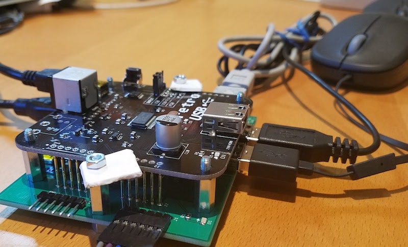
I developed the Wombat tester (pictured above with a Wombat riding on top) back in 2017. It’s a board with some simple electronics and an array of spring-loaded pogo pins that make contact with a Wombat board placed on top of it. Grab a newly-assembled Wombat, press it down onto the bed of pins, press a button, and in a few seconds you’ll have a functional test result. Hooray for high-speed testing. The Wombat tester that’s used by the Chinese factory is the original one that I hand-built six years ago.
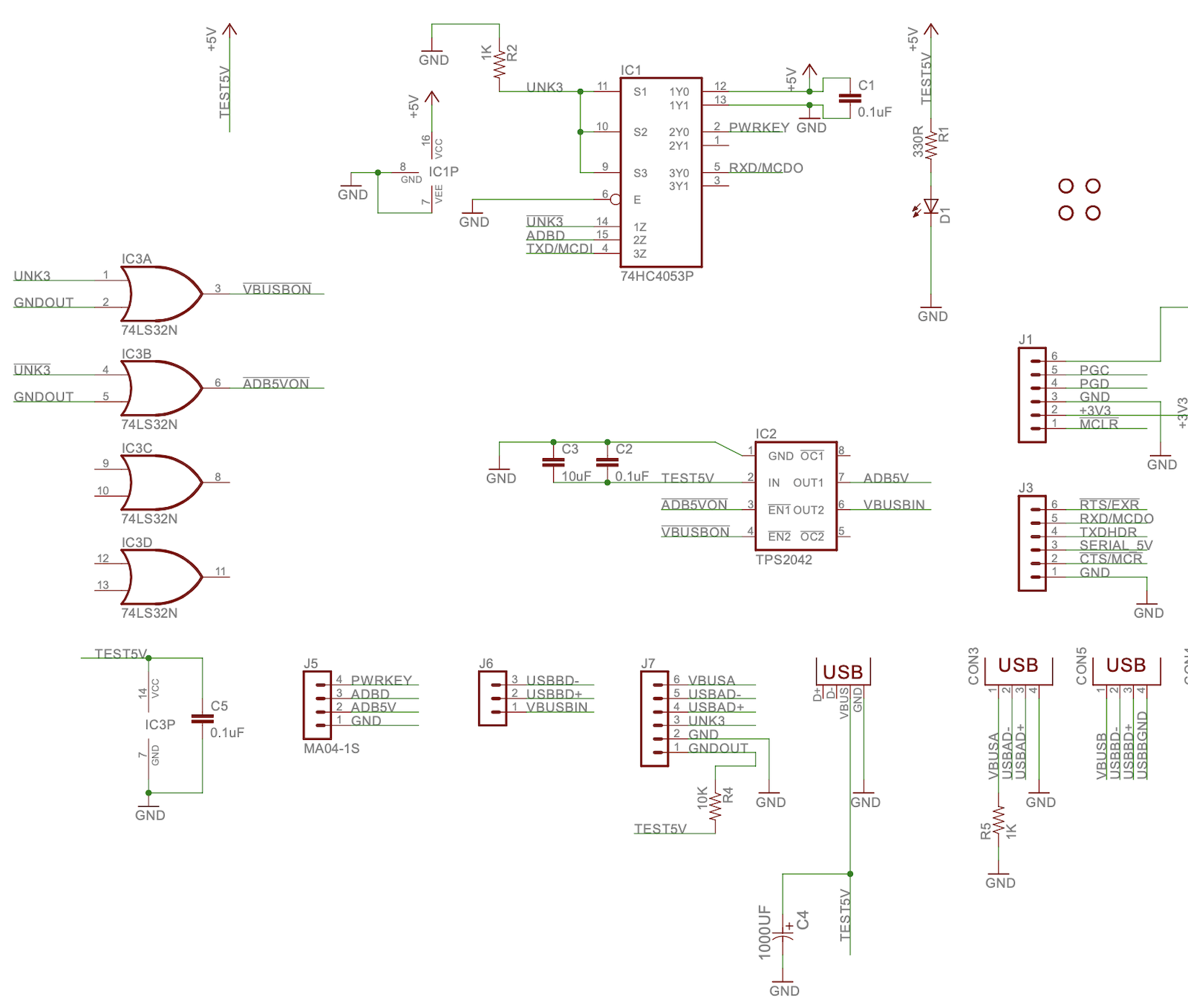
The tester’s schematic is terrible, and I have no one to blame but myself. It looks like a pile of disconnected components where you can’t really make sense of anything. There are only three chips – everything else is connectors or pogo pins. IC1 is a triple 2-channel analog switch, IC2 is a power distribution switch, and IC3 is a simple quad-OR:
I had only two pieces of information:
- The functional test was failing ADB communication. USB communication was apparently OK.
- An engineer found that bridging pins 6 and 7 on IC2 allowed the test to finish successfully.
The engineer suspected IC2 had failed and was searching for a replacement. Given the clues and the schematic diagram, what do you think is the most likely cause of the failure?
IC2 pins 6 and 7 are two separate power supplies: one that’s normally supplied by the ADB host, and another that’s supplied by the USB host. Only one should be active at a time, so bridging them together is not a valid test. Because bridging helped the failing ADB test to succeed, it suggested maybe the ADB5V supply was not turning on when it should. Yes, that could be due to IC2 failure, but could also have other causes.
The ADB5V supply is enabled by the control signal /ADB5VON at IC2 pin 3. That signal comes from the quad-OR gate at IC3, so maybe that was the source of failure? The quad-OR is also responsible for generating the USB power supply control signal. Both signals are dependent on three signals named UNK3, /UNK3, and GNDOUT. Because bridging the IC2 supply pins helped somehow, we can probably conclude the USB supply was active, meaning that /VBUSBON had to be asserted. If the quad-OR was working correctly, that means UNK3 and GNDOUT both must have been low.
What’s with these UNK3 and /UNK3 signals? Tracing back further, we see that /UNK3 is generated form IC1, where one channel of the analog switch is rigged up to behave like an inverter. The non-inverted signal UNK3 has a pull-down resistor at R2. Ultimately the UNK3 signal comes from J7 pin 3, which is one of the pogo pins. The signal comes from the Wombat board being tested, via the pogo pin.
Hmm… what would happen if that pogo pin were misaligned or broken? UNK3 would be disconnected and floating, but the R2 pull-down resistor would bring it low. With GNDOUT also low, /VBUSBON would always be asserted and /ADB5VON would never be asserted. The ADB power supply would never turn on, the USB supply would always be on, and the behavior would be consistent with the observed clues.
Mulling this analysis over a cup of coffee, I replied to the factory: “Check if pogo pin 3 at J7 is bent”. Their response came the next day: “Steve, you are really a professional engineer! The guess you made is correct. After trying again, the tester board started working normally.”
Success! That was a very satisfying fix, based on minimal information and without physical access to the faulty circuit.
Read 1 comment and join the conversation1 Comment so far
Leave a reply. For customer support issues, please use the Customer Support link instead of writing comments.
I make lots of similar jigs for my projects and boards that I design. Some more complex than others. The pogo pins have a notch in the middle that stops the plunger from coming out. That is a weak point and common failure point. Also the bottom where you solder the pins is a common fail point.
So what I do, is I use a 2nd blank jig PCB that is placed around or better – *above* that notch in the pins. This 2nd pcb is spaced evenly using other PCB scraps or whatever makes sense to allow the 2 PCBs to be perfectly parallel. Sometimes I solder the pogos in the top PCB as well at opposite/diagonal corners for better support as well. This approach allows the pins to also be perfectly parallel to one another and never shift out of position. After thousands of tests a pogo might still fail and that’s easy enough to spot and replace.