

Archive for the 'Bit Bucket' Category
Transistor Puzzles
![]()
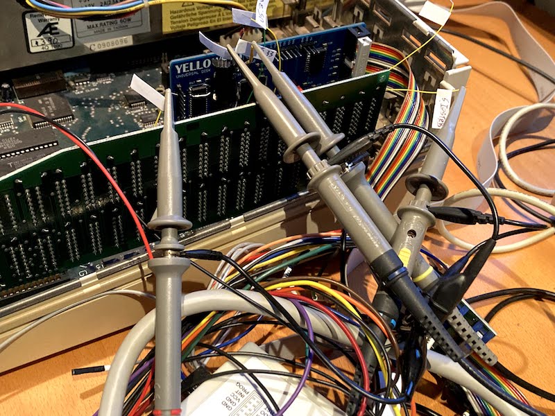
I’ve fallen into a deep hole involving current-limiting circuits and current sources, in an attempt to solve a minor problem with the Yellowstone disk controller. In the big scheme of things, this isn’t a very important problem, but it has me intrigued. I’ve created a simulation of a circuit that may solve the problem, but it exhibits some transistor behavior that I don’t understand. Specifically, the base currents of the transistors don’t seem to follow the rules that I thought I understood.
You can see a working simulation of the circuit here.
The are two SPDT switches at the top of the diagram, representing Yellowstone’s two disk connectors. On pin 9 of this connector, some types of drives will have a 10K resistor connected to the +12V supply. This type of drive needs a -12V supply input on pin 9. It will use about 3 mA at most from -12V. Other types of drives will have a direct connection to +5V on pin 9 (+5V is also provided on pin 11 to all drive types). Yellowstone can either provide an additional +5V supply on pin 9 for this type of drive, or more simply, just leave the pin unconnected.
The basic idea here is to establish a current limiter of about 10-20 mA for pin 9. That’s more than enough for normal operation with the -12V supply, and it prevents dangerously high amounts of current flowing if -12V is directly connected to +5V as in the second type of drive.
Here’s the puzzle: the three NPN transistors have all their bases connected, and all their emitters connected. As shown, they all have the same base-emitter voltage Vbe of 0.668 volts. My mental model is that the base-emitter connection is essentially like a diode. With identical diodes, identical Vbe, and a single shared 470 ohm current-limiting resistor, I would expect the base current Ib to be identical for all three transistors. Yet they’re not. The middle transistor’s Ib is 7.2 mA while the others are only 0.165 mA.
The fact that one transistor is in saturation must be relevant. But the “base-emitter connection is a diode” assumption is failing here, and I can’t explain why. I need to read more transistor theory.
Read 13 comments and join the conversationYellowstone Glitch, Part 7: Maybe a Conclusion
All these Yellowstone glitching mysteries may finally be headed for a conclusion. It looks like there are at least two separate problems with different causes: one causing glitching during a bus cycle and the other causing glitching at the end of a bus cycle.
Fighting at End of Bus Cycles?
This one is complicated to explain, so bear with me. You should understand that the Apple IIgs is a 5V system, but Yellowstone uses a 3.3V 74LVC245 to communicate on the data bus. This works because the LVC family is 5V tolerant on its inputs, and its 3.3V output is high enough to be sensed as a valid “high” by 5V logic chips. On the IIgs motherboard there’s a 74HCT245 that handles the computer’s side of transfers to and from the data bus.
Yesterday I noticed something curious: when Yellowstone is driving a 3.3V high value onto the data bus, at the end of the bus cycle the voltage always immediately jumps up to 5V, and stays there for a few hundred nanoseconds until something else puts a value on the pus. What’s doing that? Is there a 5V pull-up resistor on the bus, or something similar? No. When Yellowstone is driving a 0V low value onto the data bus, the voltage remains at 0V after the end of the bus cycle.
I’m not 100 percent sure, but I think at the end of a bus cycle the IIgs is immediately reversing the direction of its 74HCT245. Previously this chip was taking the peripheral card’s data from the peripheral slot data bus and moving it to an internal data bus, but now it begins taking data from the internal data bus and moving it to the peripheral slot data bus. And what data is that? In the first tens of nanoseconds after the direction is reversed, it’s actually the same data that the peripheral card was outputting, now briefly stored in the bus capacitance of the internal data bus.
What happens if the peripheral card’s output driver is a bit slow to turn off at the end of a bus cycle, due to propagation delays on the control signals? Since the peripheral card and the 74HCT245 from the IIgs are both driving the same data onto the bus, normally it should be OK. But for Yellowstone and its 3.3V 74LVC245, it’s not OK. For a time of roughly 15 ns, it causes 5V and 3.3V sources to both try to drive the bus at the same time, resulting in high current flows into the 3.3V supply, and overall badness. This is what I strongly suspect is causing Yellowstone’s end-of-cycle spikes and glitching.
There are several possible solutions:
- adjust Yellowstone’s ‘245 turn-off so it happens earlier, before the bus cycle is theoretically over
- modify Yellowstone to use a true 5V output driver, so there’s no 3.3V-to-5V conflict
- insert series resistors on the data bus to limit the current from 3.3V-to-5V conflict to safe levels
I implemented option 1, and it substantially reduced the spikes at the end of bus cycles. Surprisingly, it didn’t eliminate them completely. It feels strange to disable the ‘245 before the bus cycle is over, because the CPU doesn’t capture the bus value until the very end of the cycle. It seems like it should cause bad data to be read, causing malfunctions. But in practice it appears to work OK, probably thanks to that bus capacitance persisting the data value even after the ‘245 shuts off.
I also implemented option 2, through a bit of board surgery in which I replaced Yellowstone’s 74LVC245 with a dual-supply 74LVC8T245. This almost completely eliminated the spikes at the end of bus cycles, because the voltage on the bus stays constant at 5V after the cycle ends.
I would like to try option 3, but that will take more effort to set up.
High Current During Bus Cycles?
The second problem is the one I was chasing initially: spikes and glitches during a bus cycle, at the moment when the 74LVC245 is enabled and begins driving the data bus. I had a theory this was caused by a brief violation of the max output voltage spec of the 74LVC245, when it tries to output 3.3V but finds the bus capacitance is already charged to 5V. So I desoldered the 74LVC245 and replaced it with a 74LVT245, a nearly identical chip but with a higher max output voltage spec above 5V. Unfortunately this did nothing to help the spikes and glitches during bus cycles. Then I replaced the 74LVT245 with a 74LVC8T245, a dual-voltage chip with true 5V I/O on the Apple II side. Again this did nothing to solve the problems during bus cycles.
Based on these two tests, I concluded that violating the max output voltage spec of the 74LVC245 was never a problem, or at least it was never the main problem. The signal spikes are very likely caused by a large amount of current briefly flowing when all the data bus outputs change simultaneously from 1 to 0 or vice-versa. This is a “normal” condition, not a violation, but it’s troublesome. I’ve attempted several board modifications to help meet this sudden current demand, including adding a 10 uF bypass capacitor to the ‘245, and adding extra power and ground wires from the ‘245 straight back to the voltage regulator. None of it seemed to help.
I can’t quite explain this, since I didn’t think there should really be all that much current flowing. I guess I was wrong. But the only solution seems to be finding ways to reduce the current, or spread it out over a longer period of time. That’s what my 10101010 pre-driving trick accomplishes, but there’s plenty more room for reducing the current further.
Some possible options here:
- replace the 74LVC245 bidirectional buffer with two unidirectional buffers: an LVC buffer for input and an LS buffer for output
- insert series resistors on the data bus to limit the current
- something else I’m overlooking
The 74LS245 is an appealing option because the LS family just can’t drive very hard, at least not when outputting a high voltage. But it won’t work as a bidirectional substitute for the 74LVC245, because its 5V outputs (or close enough to 5V) would damage the FPGA. So I’d need to use the LS chip for output only, and use an LVC chip for input. That’s not very appealing. I’m also not sure how well it would reduce the current when driving low voltages instead of high ones. It might still draw too much current, or it might be fine. Isn’t this basically how all 1980s vintage peripheral cards worked? How did they avoid this problem?
Options 1 and 2 should both resolve the problems at the end of the bus cycle too, so that’s good. The other alternatives have more limited application. Adjusting the ‘245 turn-off timing does nothing to help the problems during the bus cycle, nor does using a 74LVC8T245 chip.
Unsolved Mysteries
Sadly none of the above can explain why these same problems didn’t appear in revision 1 of Yellowstone. Probably they did, but they weren’t severe enough to cause bit flips and malfunctions, so I never noticed. The only partial explanation I can think of is that revision 2’s RAM chip is to blame. Revision 1 used internal FPGA RAM and didn’t have a separate RAM chip. My guess is that the extra current used by the RAM is exacerbating the problem somehow.
Next Steps?
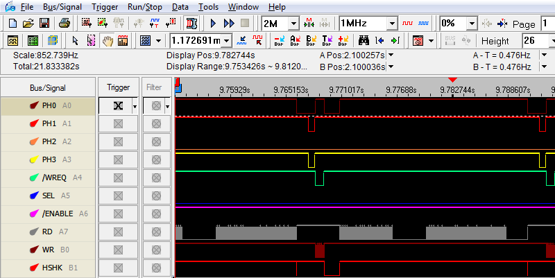
If you’re still reading this wall of text, it’s time to evaluate the possible solutions and make a choice. Let’s start with the simplest option: do nothing (at least from a hardware standpoint). By implementing the 10101010 pre-driving trick, adjusting the ‘245 turn-off timing, and a few other small timing changes, I’ve already improved things enough to get my prototype board working.
Here’s what things look like with only the FPGA logic changes. Same as in part 6, the traces shown are:
- Blue (Ch4) is address line A1. It’s a 5V input from the Apple II
- Yellow (Ch1) is the 3.3V supply voltage, measured at the VCC pin of the ‘245.
- Cyan (Ch2) is IOSTROBE, and marks the boundaries of the bus cycle.
I didn’t capture GND this time.

Yeah it still doesn’t look great, but it works. If you’ve forgotten how bad everything looked before I made the FPGA logic changes, here’s the headline image again from part 6:

So maybe this is good enough now, without needing further hardware changes? Especially if some of the ringing shown in the scope traces is due to my poor probe setup rather than being a true representation of the signal?
If a hardware change is needed, series resistors are attractive because they’re simple and easy. But what value of resistor? It must be big enough to significantly limit the current in a bus-fighting scenario, but not so big that it results in failure to meet the Vil and Vih specs of the other chips on the data bus that are receiving data.
Let’s say I used 100 ohm series resistors. In a 3.3V-to-5V bus fighting scenario at the end of a bus cycle, that would limit the current to 1.7 / 100 = 17 mA per data bus line, or 136 mA total. That’s still pretty high. Too high, I think.
If I used 500 ohm resistors, it would limit the total current to a much more modest 27.2 mA total, but it would create a new problem. For the 74LS family inputs on the data bus of the Apple IIe, and for as many as six other peripheral cards installed that use 74LS parts, the inputs source 0.2 mA when they’re “receiving” a logical low value. All combined that’s 1.4 mA worst case. With 500 ohm resistors and a current of 1.4 mA, even if Yellowstone could output a true 0.0V logical low value, the LS inputs would see a voltage of 1.4 * 500 = 0.7V, which is almost above the Vil threshold for 74LS family parts. In short, with a fully loaded set of 7 peripheral cards that all use 74LS logic, and 500 ohm resistors, Yellowstone might not work.
There’s some middle ground here. Resistor values from roughly 150 to 500 could probably work to solve both problems, but it’s a narrow enough range that it makes me slightly nervous. Maybe go with 220 or 330 ohm.
If a hardware change is needed but series resistors won’t do, then I think the only viable alternative is a two-chip solution with 74LS output and 74LVC input. But I don’t love this solution, for the reasons mentioned previously: extra chips, extra design complexity, and a concern it might not work anyway for driving a logical low voltage. There would be a small amount of additional control complexity too. Each chip would need a separate enable signal from the FPGA, where spare pins are scarce, and extra care would be needed to prevent enabling both at once.
Some other combination of solutions might be possible too, like 74LVC8T245 with series resistors. But I don’t want to go overboard.
As you might expect, I’ve grown very tired of this glitching problem, and my enthusiasm for further tests and experiments is low. My gut says to accept the software-only solution and call it good, or else maybe to add series resistors. But I don’t want to sweep this problem under the rug, only to have it reappear later in rare circumstances I can’t troubleshoot. If you were me, what would you do?
Read 15 comments and join the conversationNASA Struggles to Fix Hubble Space Telescope’s 1980s Computer

Did anybody else see this week’s news about problems with Hubble’s 80s-vintage onboard computer and think: *gasp* My moment in life has arrived! Hold my beer.
“Hello, NASA? Did you guys try PR#6? Sometimes the boot disk gets dust on it; ask an astronaut to blow it off and then reboot. Hello? Hello? Why did they hang up?”
The Hubble’s computer is actually an NSSC-1, an 18-bit machine with 64KB memory. The version on Hubble is likely built from a few dozen discrete MSI chips. There are two fully redundant computers on board, and four independent 64KB memory modules, any of which can be enabled or disabled from the ground in the event of a problem. But 30 years of bombardment by cosmic rays will take a toll on the hardware.
Be the first to comment!When A Space Is Not A Space
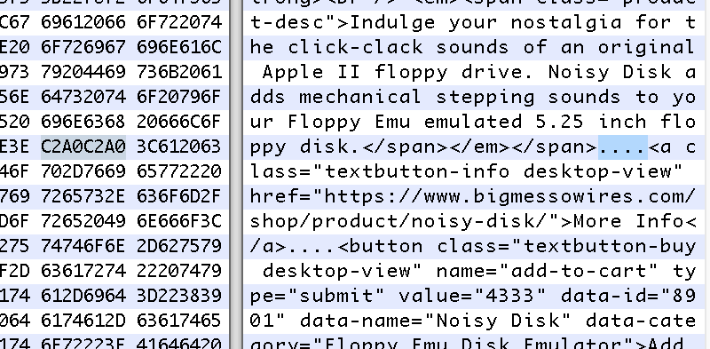
I just spent more than two hours troubleshooting a seemingly simple HTML problem. When I copied and pasted a small section of HTML, the web browser displayed the newly-pasted section differently from the original. The horizontal spacing between some of the elements was slightly different, causing the whole page to look wrong. But how could this be? The two HTML sections were identical – the new one was literally a copy of the old one.
This simple-sounding problem defied all my attempts to explain it. I came up with lots of great theories: problems with my CSS classes, or with margins and padding. Mismatched HTML tags. Browser bugs. I tried three different browsers and got the same results in all of them.
Feeling very confused, I looked again at the two sections of HTML in the WordPress editor (text view), and confirmed they were exactly identical. Then I tried Firefox’s built-in web developer tools to view the page’s rendered elements, and compared all their CSS properties. Identical – yet somehow they rendered differently. I used the developer tools to examine the exact HTML received from my web server, checked the two sections again, and verified they were character-for-character identical. Firefox’s “page source” tool also confirmed the two sections were exactly identical.
By this point I was getting ready to blame cosmic rays or voodoo magic. I discovered that any time I copy-pasted any similar HTML section, the newly-pasted section would appear in the browser with the wrong element spacing. How could this possibly be? I then tried the W3C Validator, which found some other problems with my page, but nothing that could explain this behavior. And once again, it confirmed that despite rendering differently in the browser, the two sections of HTML were identical.
Clearly something wasn’t adding up. I used curl to download the web page from my web server, viewed the local copy, and saw the same behavior as before. But when I opened the stored .html document with a hex editor, I finally had my answer. The two sections of HTML were not identical: one section used a different type of space character from the other.
What the hell.
I discovered that the original HTML section contained non-breaking spaces. But instead of encoding them with the entity, they were encoded directly as Unicode character C2A0. I’m not sure when or how this happened, but I blame WordPress. When viewing this section in the WordPress HTML editor, the C2A0 spaces appeared like normal spaces, and copy-pasting the section inside the editor silently converted non-breaking spaces to normal spaces with hex value 20. So the copied version rendered differently, even though the source HTML appeared to be the same.
This is like the 21st century version of confusing a zero with a capital letter O, yet worse. I wasn’t even aware that non-breaking spaces have a Unicode character value – I thought was the only way to encode them. I changed the HTML back to use and now it all works fine.
I’m surprised at how many different tools failed to reveal this subtle but important difference between types of spaces in the HTML source. The WordPress HTML editor failed to show or correctly handle the difference. The Firefox web developer tools and page source tools failed. The W3C Validator’s source view failed. Curl plus a hex editor was the only way to finally establish the ground truth about the precise contents of the HTML source.
Read 9 comments and join the conversationFPGA Block RAM Packing
In an earlier blog post, I was lamenting how one-ninth of an FPGA block RAM was wasted when storing 8-bit ROM data, because there’s no simple way to make use of the 9th parity bit in each word of a block RAM. Horrors! To fight this injustice, I’ve developed a solution that I call packed ROM. It stores nine 8-bit bytes in eight 9-bit words of block RAM, and provides an interface to read the data as if it were an 8-bit memory with a larger depth. Using this method, I’m able to store 1152 bytes of read-only data per block RAM instead of only 1024. The solution relies on the fact that the block RAMs are dual port – you can read from two different addresses simultaneously. Compared with using the same number of block RAMs as a standard 8-bit wide ROM, this solution consumes an extra 54 LUT4s in a MachXO2-1200 FPGA – about 4 percent of the total. It increases the MachXO2-1200’s effective capacity for this type of 8-bit ROM data from 7168 to 8064 bytes.
Here’s the Verilog code, as well as a Python program that reads a plain binary file and writes a “packed” file in .mem format. The code assumes 7 block RAMs, but should be easily adaptable to other numbers.
module packedROM #(parameter NUM_BLOCK_RAMS = 7) (
    input [12:0] addr,
	input clk,
	output reg [7:0] Q
    );

	// packs 1152*NUM_BLOCK_RAMS 8-bit data bytes into 1024*NUM_BLOCK_RAMS 9-bit words
	// uses 54 LUT4s of the MachXO2
	// may need to change addr width depending on NUM_BLOCK_RAMS. Use $clog2()?

	// nine bytes A-I are packed into eight 9-bit words as follows:
	// 0: I3 I2 I1 I0 A4 A3 A2 A1 A0
	// 1: I7 I6 I5 I4 B4 B3 B2 B1 B0
	// 2: F7 F6 E7 E6 C4 C3 C2 C1 C0
	// 3: H7 H6 G7 G6 D4 D3 D2 D1 D0
	// 4: A7 A6 A5 E5 E4 E3 E2 E1 E0
	// 5: B7 B6 B5 F5 F4 F3 F2 F1 F0
	// 6: C7 C6 C5 G5 G4 G3 G2 G1 G0
	// 7: D7 D6 D5 H5 H4 H3 H2 H1 H0
	// bytes A-H are sequental in the byte-oriented address space below addr 1024*NUM_BLOCK_RAMS
	// byte I is one of the "extra" bytes, in byte-oriented address space beyond addr 1024*NUM_BLOCK_RAMS

	reg [12:0] wordAddressA;
	reg [12:0] wordAddressB;

	wire [8:0] QA;
	wire [8:0] QB;

	// dualPortROM is a wrapper for the MachXO2 block RAMs, created by the Lattice IP Express tool.
	// it is actually a dual port RAM with the write input unused
	dualPortROM myDualPortROM(
		.DataInA(9'b000000000),
		.DataInB(9'b000000000),
		.AddressA(wordAddressA),
		.AddressB(wordAddressB),
		.ClockA(clk),
		.ClockB(clk),
		.ClockEnA(1'b1),
		.ClockEnB(1'b1),
		.WrA(1'b0),
		.WrB(1'b0),
		.ResetA(1'b0),
		.ResetB(1'b0),
		.QA(QA),
		.QB(QB)
	);

	wire [12:0] overflowAddr = addr - (NUM_BLOCK_RAMS * 1024);

	always @* begin
		if (addr < NUM_BLOCK_RAMS * 1024) begin
			// packed area, bytes A-H
			wordAddressA <= addr;
			// word address for the upper bits depends on low three bits of the byte address
			case (addr[2:0])
				0: begin // A
					wordAddressB <= { addr[12:3], 3'b100 };
					Q <= { QB[8:6], QA[4:0] };
					end
				1: begin // B
					wordAddressB <= { addr[12:3], 3'b101 };
					Q <= { QB[8:6], QA[4:0] };
					end
				2: begin // C
					wordAddressB <= { addr[12:3], 3'b110 };
					Q <= { QB[8:6], QA[4:0] };
					end
				3: begin // D
					wordAddressB <= { addr[12:3], 3'b111 };
					Q <= { QB[8:6], QA[4:0] };
					end
				4: begin // E
					wordAddressB <= { addr[12:3], 3'b010 };
					Q <= { QB[6:5], QA[5:0] };
					end
				5: begin // F
					wordAddressB <= { addr[12:3], 3'b010 };
					Q <= { QB[8:7], QA[5:0] };
					end
				6: begin // G
					wordAddressB <= { addr[12:3], 3'b011 };
					Q <= { QB[6:5], QA[5:0] };
					end
				7: begin // H
					wordAddressB <= { addr[12:3], 3'b011 };
					Q <= { QB[8:7], QA[5:0] };
					end
			endcase
		end
		else begin
			// overflow area, byte I
			// word address is byte overflow address times 8 for the lower bits, and times 8 plus 1 for the upper bits
			wordAddressA <= { overflowAddr[9:0], 3'b000 };
			wordAddressB <= { overflowAddr[9:0], 3'b001 };
			Q <= { QB[8:5], QA[8:5] };
		end
	end
endmodule


import os
from array import array

infile = "coderom.bin"
outfile = "coderom.mem"

inputData = array('B')

insize = os.path.getsize(infile)
with open(infile, 'rb') as f:
    inputData.fromfile(f, insize)
    out = open(outfile,"w")

    num_block_rams = 7
    outsize = 1024 * num_block_rams

    for x in range(0,outsize):
        baseAddr = x & ~7
        if x & 7 == 0:
            out.write('{:02X}\n'.format( (((inputData[outsize+baseAddr//8])&0xF)<<5) | ((inputData[baseAddr])&0x1F)))
        elif x & 7 == 1:
            out.write('{:02X}\n'.format( (((inputData[outsize+baseAddr//8])&0xF0)<<1) | ((inputData[baseAddr+1])&0x1F)))
        elif x & 7 == 2:
            out.write('{:02X}\n'.format( (((inputData[baseAddr+5])&0xC0)<<1) | (((inputData[baseAddr+4])&0xC0)>>1) | ((inputData[baseAddr+2])&0x1F)))
        elif x & 7 == 3:
            out.write('{:02X}\n'.format( (((inputData[baseAddr+7])&0xC0)<<1) | (((inputData[baseAddr+6])&0xC0)>>1) | ((inputData[baseAddr+3])&0x1F)))
        elif x & 7 == 4:
            out.write('{:02X}\n'.format( (((inputData[baseAddr])&0xE0)<<1) | ((inputData[baseAddr+4])&0x3F)))
        elif x & 7 == 5:
            out.write('{:02X}\n'.format( (((inputData[baseAddr+1])&0xE0)<<1) | ((inputData[baseAddr+5])&0x3F)))
        elif x & 7 == 6:
            out.write('{:02X}\n'.format( (((inputData[baseAddr+2])&0xE0)<<1) | ((inputData[baseAddr+6])&0x3F)))
        elif x & 7 == 7:
            out.write('{:02X}\n'.format( (((inputData[baseAddr+3])&0xE0)<<1) | ((inputData[baseAddr+7])&0x3F)))
Read 4 comments and join the conversation
UDC: The Next Generation
I’m still working on development of a disk controller card for the Apple II. As part of that effort, I’m still trying to understand the design of the UDC disk controller. My hope is to combine what I learn about the UDC, the Liron disk controller, and the standard Disk II controller in order to build something with the best qualities of all three. But for now I’m deep in the weeds with the UDC, and today I was pleased to finally confirm my long-held theory about UDC support for intelligent Smartport drives!
In the Apple II world, there are three primary types of disk drives: 5.25 inch drives, dumb 3.5 inch drives, and intelligent drives using the Smartport protocol. The best-known example of an intelligent Smartport drive is the Unidisk 3.5, but others include Floppy Emu’s emulated Smartport Hard Disk.
For quite a while now, I’ve been chasing after this question of whether the UDC supports intelligent Smartport drives. The two available UDC manuals are slightly vague, but could be interpreted as saying there’s no support. Several sources on the web say Smartport drives aren’t supported, and you’ll damage your drive or UDC card if you try. But a contemporary print ad for the UDC advertises Unidisk 3.5 compatibility. I looked at ROM dumps from several different UDC versions, and found what looked like Smartport-related code in some older ones but not in newer ones. It’s all very confusing.
Fun With ROM Hacking
After a month of theory and research, I finally got to try some hands-on tests. The original UDC card is called the “long” version, and the follow-up card with a custom ASIC is the “short” version. I’ve been unable to find anyone with a long UDC (call me!), but I was able to borrow a short UDC. I spent a while mapping all the connections on the card and constructing a schematic, until I was satisfied there were no lurking dangers from merely connecting a Smartport drive to it. I connected a Floppy Emu configured for Smartport emulation mode, booted it up, and… it did nothing. Then I connected a Unidisk 3.5 and tried again, and it also did nothing. Blah.
This UDC short card came with version 4.0 of the ROM, which I’d previously analyzed and concluded didn’t contain any code for Smartport drive support. So it’s not surprising that it didn’t work, but I’d hoped maybe I’d missed something in my ROM analysis. My earlier analysis of ROM version 2.3 from the long UDC found that it did contain code for Smartport drives. I strongly suspect the short UDC is functionally identical to the long, despite its different physical appearance. So what happens if you take ROM 2.3 from a long UDC, and stick it in a short UDC card? Let’s find out!
The ROM is stored in a 27C64 EPROM and is socketed, so no modifications were necessary on the UDC card. I used a 28C64 EEPROM as a drop-in replacement, and programmed it with ROM version 2.3 using my EasyPro universal programmer. (Coincidence: this EasyPro 90B programmer was first mentioned on this blog precisely 13 years ago today. I feel very, very old.) I unsocketed the original ROM chip, popped in the new one, booted up, and… it did nothing. Worse than nothing, it actually froze up the computer. I checked the disk I/O signals with a logic analyzer, and there was no activity at all. Blah again.
Feeling disappointed, I gave up. The next morning, I noticed that the logic analyzer wasn’t actually connected. Oops.
After I’d fixed that, I could clearly see evidence of a Smartport reset and initialization sequence on the disk I/Os, but it still wasn’t working. Eventually I concluded that the code in the ROM was crashing or getting stuck in an infinite loop somewhere. But where, and why? I would have tried single-stepping through the code, but quickly discovered that’s extremely difficult for code in ROM on an Apple IIe.
By carefully comparing the ROM 4.0 and ROM 2.3 code, eventually I was able to guess the problem. A key feature of the UDC is that it sometimes pulls the 6502’s RDY input low to temporarily halt the CPU. This is a sort of flow control mechanism, and happens whenever the code tries to read a byte from the disk, but a new byte isn’t available yet. It appears that the details surrounding use of RDY changed between the long and short UDC, and the short version will halt the CPU on reads to some memory locations that the long UDC ignores. By comparing the two ROMs and making some educated guesses, I was able to modify the version 2.3 ROM so that it no longer caused the short UDC to freeze the computer. But it still didn’t work. Blah for a third time.
After more tinkering and head-scratching, I disconnected the Floppy Emu and tried the Unidisk 3.5 again. I was amazed when it booted right up! But now I had a new puzzle to solve, to explain why the Unidisk 3.5 worked but Floppy Emu’s Smartport emulation didn’t, even when using the exact same disk.
The logic analyzer eventually revealed the answer. Something like 5-10% of the data packets from the Unidisk 3.5 were NAK’d by the UDC card, forcing them to be retransmitted. Some packets had to be retransmitted multiple times. In all my time tinkering with the Smartport protocol over the years, I’ve never before seen a NAK of valid data, and Floppy Emu doesn’t even implement retransmitting a packet in case of a NAK. I implemented the missing retransmit logic, and the Floppy Emu worked! Hooray!
The mystery still wasn’t completely solved, however. What was causing some packets to be NAK’d, from both the Floppy Emu and a real Unidisk 3.5? The NAK rate was also much higher with the Floppy Emu than with the Unidisk 3.5, approaching 30-50%. Acting on a hunch, I experimented with small changes to the Floppy Emu’s bit rate, and found that it caused some changes in the NAK rate, but the results weren’t conclusive.
The “correct” bit rate is either one bit every 4.0 microseconds, or every 3.96 microseconds, depending on your reference source and your assumptions. Floppy Emu with the latest firmware does one bit every 3.95 us. I found that at 4.2 us I got a 100% NAK rate, but at 4.1 us the NAK rate suddenly dropped to about 10%, and at 4.05 us and 4.0 us the NAK rate grew worse again. That doesn’t really make sense, and I didn’t repeat the tests enough times to be very confident in those results. My suspicion is that either the UDC short card is very sensitive to small changes in bit rate, or else that substituting the long UDC ROM is negatively affecting the behavior somehow. I’m not sure it’s worth chasing this mystery further, since it’s quite possibly caused by my weird hybrid card setup.
So the $64000 question is finally answered, sort of. The standard short UDC card does not support Smartport drives, but connecting one won’t damage anything. But it does support Smartport drives when using an appropriately hacked-up ROM, proving that it’s entirely a question of software rather than hardware. As for the long UDC, I still can’t say for certain without examining one directly, but all the evidence points to it supporting Smartport drives.
Where to Next?
This probably marks the end of my very long detour into “how does the UDC work?” and a return to actual development on my disk controller card. Next step: see if I can duplicate the UDC behavior (or something close to it) with my FPGA-based approach.
Read 7 comments and join the conversation