

Yellowstone Glitch, Part 7: Maybe a Conclusion
All these Yellowstone glitching mysteries may finally be headed for a conclusion. It looks like there are at least two separate problems with different causes: one causing glitching during a bus cycle and the other causing glitching at the end of a bus cycle.
Fighting at End of Bus Cycles?
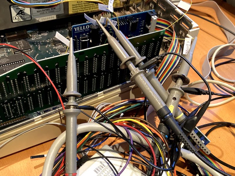
This one is complicated to explain, so bear with me. You should understand that the Apple IIgs is a 5V system, but Yellowstone uses a 3.3V 74LVC245 to communicate on the data bus. This works because the LVC family is 5V tolerant on its inputs, and its 3.3V output is high enough to be sensed as a valid “high” by 5V logic chips. On the IIgs motherboard there’s a 74HCT245 that handles the computer’s side of transfers to and from the data bus.
Yesterday I noticed something curious: when Yellowstone is driving a 3.3V high value onto the data bus, at the end of the bus cycle the voltage always immediately jumps up to 5V, and stays there for a few hundred nanoseconds until something else puts a value on the pus. What’s doing that? Is there a 5V pull-up resistor on the bus, or something similar? No. When Yellowstone is driving a 0V low value onto the data bus, the voltage remains at 0V after the end of the bus cycle.
I’m not 100 percent sure, but I think at the end of a bus cycle the IIgs is immediately reversing the direction of its 74HCT245. Previously this chip was taking the peripheral card’s data from the peripheral slot data bus and moving it to an internal data bus, but now it begins taking data from the internal data bus and moving it to the peripheral slot data bus. And what data is that? In the first tens of nanoseconds after the direction is reversed, it’s actually the same data that the peripheral card was outputting, now briefly stored in the bus capacitance of the internal data bus.
What happens if the peripheral card’s output driver is a bit slow to turn off at the end of a bus cycle, due to propagation delays on the control signals? Since the peripheral card and the 74HCT245 from the IIgs are both driving the same data onto the bus, normally it should be OK. But for Yellowstone and its 3.3V 74LVC245, it’s not OK. For a time of roughly 15 ns, it causes 5V and 3.3V sources to both try to drive the bus at the same time, resulting in high current flows into the 3.3V supply, and overall badness. This is what I strongly suspect is causing Yellowstone’s end-of-cycle spikes and glitching.
There are several possible solutions:
- adjust Yellowstone’s ‘245 turn-off so it happens earlier, before the bus cycle is theoretically over
- modify Yellowstone to use a true 5V output driver, so there’s no 3.3V-to-5V conflict
- insert series resistors on the data bus to limit the current from 3.3V-to-5V conflict to safe levels
I implemented option 1, and it substantially reduced the spikes at the end of bus cycles. Surprisingly, it didn’t eliminate them completely. It feels strange to disable the ‘245 before the bus cycle is over, because the CPU doesn’t capture the bus value until the very end of the cycle. It seems like it should cause bad data to be read, causing malfunctions. But in practice it appears to work OK, probably thanks to that bus capacitance persisting the data value even after the ‘245 shuts off.
I also implemented option 2, through a bit of board surgery in which I replaced Yellowstone’s 74LVC245 with a dual-supply 74LVC8T245. This almost completely eliminated the spikes at the end of bus cycles, because the voltage on the bus stays constant at 5V after the cycle ends.
I would like to try option 3, but that will take more effort to set up.
High Current During Bus Cycles?
The second problem is the one I was chasing initially: spikes and glitches during a bus cycle, at the moment when the 74LVC245 is enabled and begins driving the data bus. I had a theory this was caused by a brief violation of the max output voltage spec of the 74LVC245, when it tries to output 3.3V but finds the bus capacitance is already charged to 5V. So I desoldered the 74LVC245 and replaced it with a 74LVT245, a nearly identical chip but with a higher max output voltage spec above 5V. Unfortunately this did nothing to help the spikes and glitches during bus cycles. Then I replaced the 74LVT245 with a 74LVC8T245, a dual-voltage chip with true 5V I/O on the Apple II side. Again this did nothing to solve the problems during bus cycles.
Based on these two tests, I concluded that violating the max output voltage spec of the 74LVC245 was never a problem, or at least it was never the main problem. The signal spikes are very likely caused by a large amount of current briefly flowing when all the data bus outputs change simultaneously from 1 to 0 or vice-versa. This is a “normal” condition, not a violation, but it’s troublesome. I’ve attempted several board modifications to help meet this sudden current demand, including adding a 10 uF bypass capacitor to the ‘245, and adding extra power and ground wires from the ‘245 straight back to the voltage regulator. None of it seemed to help.
I can’t quite explain this, since I didn’t think there should really be all that much current flowing. I guess I was wrong. But the only solution seems to be finding ways to reduce the current, or spread it out over a longer period of time. That’s what my 10101010 pre-driving trick accomplishes, but there’s plenty more room for reducing the current further.
Some possible options here:
- replace the 74LVC245 bidirectional buffer with two unidirectional buffers: an LVC buffer for input and an LS buffer for output
- insert series resistors on the data bus to limit the current
- something else I’m overlooking
The 74LS245 is an appealing option because the LS family just can’t drive very hard, at least not when outputting a high voltage. But it won’t work as a bidirectional substitute for the 74LVC245, because its 5V outputs (or close enough to 5V) would damage the FPGA. So I’d need to use the LS chip for output only, and use an LVC chip for input. That’s not very appealing. I’m also not sure how well it would reduce the current when driving low voltages instead of high ones. It might still draw too much current, or it might be fine. Isn’t this basically how all 1980s vintage peripheral cards worked? How did they avoid this problem?
Options 1 and 2 should both resolve the problems at the end of the bus cycle too, so that’s good. The other alternatives have more limited application. Adjusting the ‘245 turn-off timing does nothing to help the problems during the bus cycle, nor does using a 74LVC8T245 chip.
Unsolved Mysteries
Sadly none of the above can explain why these same problems didn’t appear in revision 1 of Yellowstone. Probably they did, but they weren’t severe enough to cause bit flips and malfunctions, so I never noticed. The only partial explanation I can think of is that revision 2’s RAM chip is to blame. Revision 1 used internal FPGA RAM and didn’t have a separate RAM chip. My guess is that the extra current used by the RAM is exacerbating the problem somehow.
Next Steps?
If you’re still reading this wall of text, it’s time to evaluate the possible solutions and make a choice. Let’s start with the simplest option: do nothing (at least from a hardware standpoint). By implementing the 10101010 pre-driving trick, adjusting the ‘245 turn-off timing, and a few other small timing changes, I’ve already improved things enough to get my prototype board working.
Here’s what things look like with only the FPGA logic changes. Same as in part 6, the traces shown are:
- Blue (Ch4) is address line A1. It’s a 5V input from the Apple II
- Yellow (Ch1) is the 3.3V supply voltage, measured at the VCC pin of the ‘245.
- Cyan (Ch2) is IOSTROBE, and marks the boundaries of the bus cycle.
I didn’t capture GND this time.

Yeah it still doesn’t look great, but it works. If you’ve forgotten how bad everything looked before I made the FPGA logic changes, here’s the headline image again from part 6:

So maybe this is good enough now, without needing further hardware changes? Especially if some of the ringing shown in the scope traces is due to my poor probe setup rather than being a true representation of the signal?
If a hardware change is needed, series resistors are attractive because they’re simple and easy. But what value of resistor? It must be big enough to significantly limit the current in a bus-fighting scenario, but not so big that it results in failure to meet the Vil and Vih specs of the other chips on the data bus that are receiving data.
Let’s say I used 100 ohm series resistors. In a 3.3V-to-5V bus fighting scenario at the end of a bus cycle, that would limit the current to 1.7 / 100 = 17 mA per data bus line, or 136 mA total. That’s still pretty high. Too high, I think.
If I used 500 ohm resistors, it would limit the total current to a much more modest 27.2 mA total, but it would create a new problem. For the 74LS family inputs on the data bus of the Apple IIe, and for as many as six other peripheral cards installed that use 74LS parts, the inputs source 0.2 mA when they’re “receiving” a logical low value. All combined that’s 1.4 mA worst case. With 500 ohm resistors and a current of 1.4 mA, even if Yellowstone could output a true 0.0V logical low value, the LS inputs would see a voltage of 1.4 * 500 = 0.7V, which is almost above the Vil threshold for 74LS family parts. In short, with a fully loaded set of 7 peripheral cards that all use 74LS logic, and 500 ohm resistors, Yellowstone might not work.
There’s some middle ground here. Resistor values from roughly 150 to 500 could probably work to solve both problems, but it’s a narrow enough range that it makes me slightly nervous. Maybe go with 220 or 330 ohm.
If a hardware change is needed but series resistors won’t do, then I think the only viable alternative is a two-chip solution with 74LS output and 74LVC input. But I don’t love this solution, for the reasons mentioned previously: extra chips, extra design complexity, and a concern it might not work anyway for driving a logical low voltage. There would be a small amount of additional control complexity too. Each chip would need a separate enable signal from the FPGA, where spare pins are scarce, and extra care would be needed to prevent enabling both at once.
Some other combination of solutions might be possible too, like 74LVC8T245 with series resistors. But I don’t want to go overboard.
As you might expect, I’ve grown very tired of this glitching problem, and my enthusiasm for further tests and experiments is low. My gut says to accept the software-only solution and call it good, or else maybe to add series resistors. But I don’t want to sweep this problem under the rug, only to have it reappear later in rare circumstances I can’t troubleshoot. If you were me, what would you do?
Read 15 comments and join the conversation15 Comments so far
Leave a reply. For customer support issues, please use the Customer Support link instead of writing comments.
I don\’t know what the capacitance is on the bus, but I think you\’re underestimating how high the switching currents can be in the absence of series resistors. The 74LVC8T245 is guaranteed to be capable of sourcing and sink 32mA per pin easily at temperatures up to 85C, and I would not be surprised if typical chips at room temperature could output twice that much momentarily when driving a capacitive load. Eight pins at 64mA each would be 512mA.
Having half of the pins initially set to 1 and half to zero would cut worst-case transient ground current by more than 50%, because the pins that are already at the correct level would help carry current that would otherwise have to go through the ground pin. There\’s a big difference between trying to drive eight pins, with no pins helping, versus trying to drive seven with one pin helping, and by the time one has four pins helping things will have improved quite a lot.
If I were designing the board, I think I\’d include series resistors, but having four inputs switching and four helping is enough of an improvement over 7+1 (which I don\’t think you had any trouble with) that I think things should probably be reliable even without the resistors.
I’ve been looking into similar issues for something I’m developing.
I’m using some 74LVC245’s too, but have been having random issues I suspect may be due to ringing/noise/poor noise immunity caused by the fast transition or prop time of the LVC logic compared to the LS logic in the rest of the system.
I found out there are things like the 74LVCR2245 which is a 74LVC245 with 22-ohm series resistors on all outputs which I will try in my case but might be helpful for you too?
Personally I’d get rid of the 3.3/5 mismatch. You’re seeing a case where that mismatch causes weirdness. I’d be worried there are others.
Disclaimer: I’ve never designed apple ][ hardware, I don’t know how common this is, etc etc
I would not be surprised if the peak currents through the ground pin are exceeding +/-500mA when switching 0x00 to 0xFF or vice versa. Precharging the bus so four bits are high and four are low will be a robust solution if the only problematic transitions involve switching all eight bits since not only will there only be half as many pins switching, but pins that are either already at the correct state or switching in the opposite direction will help share the load from the ground pin.
What do the Apple expansion interface specs specify about maximum amount a card can load the bus? It might not be a bad idea to cobble together a card which can be used as a dummy capacitive load (sitting in a slot separate from the board under dest). It probably wouldn’t be necessary to lay out a board for that–simply tack-solder some caps onto a DIP header that can go in the ROM socket of some arbitrary spare expansion board. To confirm the robustness of your design, put caps that are 8x the maximum per-slot value on four of the pins (e.g. D0, D2, D4, and D6, and test for correct operation for all sixteen combinations of initial state (0x00 or 0xFF), read value (0x00 or 0xFF), following value (0x00 or oxFF) and precharge state (0x55 or 0xAA, so the four loaded pins are driven one way and the unloaded pins the other).
If your board will work under those circumstances, I’d consider it solid. Otherwise I would think it necessary to either use resistors or lower-current driver chips.
Ooh, that 74LVCR2245 looks very appealing! I’m definitely going to try one. I wish the resistance were larger, but otherwise it looks ideal. This is a great example of not knowing what you don’t know. I never even imagined there was a part like the 74LVCR2245 so I never thought to search for one.
The 3.3V to 5V mismatch does feel slightly strange, but I think it’s pretty common in situations like this, and my tests with the 74LVC8T245 showed that using a true 5V output didn’t fix all the problems either.
I feel perpetually confused by these kinds of problems with ringing and overshoot, like no matter how many times I read about it, I never fully understand it. Like if the fast edges on a normal 74LVC are so problematic, how are people ever supposed to use them? Why aren’t I seeing the same kinds of problems internally on my PCB where other 74LVC245 chips drive inputs to the FPGA? Are designers supposed to add series resistors on every output signal from every 74LVC part everywhere? Or is it only needed for long traces, or traces with higher capacitance? What happens when your design needs to run at 250 MHz and you can’t add series resistors without blurring your signals to the point where they’re unrecognizable?
A side commentary on parts selection and assembly considerations: Yellowstone currently features five ‘245 chips, from two different families. Four of them are 74LVC245 and are connected to the Apple II data bus, address bus, and control signals. Of these four, one is bidirectional (the data bus) and the others are unidirectional. For the unidirectional ones, I could have used the unidirectional 74LVC244 instead, but I wanted to limit the number of different chip types used, and there’s no real drawback to using a bidirectional chip in a way that’s exclusively one direction.
The fifth ‘245 is a 74LS245 and is connected to the disk drive I/O signals. It’s used in one direction only. I chose a 74LS here because some of these disk I/O outputs will have pull-up resistors to 5V inside the disk drive. If I’d used a 74LVC245, I was concerned the pull-ups would cause a violation of the chip’s max output voltage rating. But if we’re talking about pull-ups to 5V that are at least 2K ohm and probably more like 10K ohm, should I really be concerned about the max output voltage issue? There would be less than 1 mA flowing the wrong way into the 3.3V power supply of the 74LVC245. My intuition is this would be OK, but I would like to hear some opinions from others. It would be great if I could simplify the Yellowstone design and use the same ‘245 family for all five chips.
Replacing the bus driver ‘245 with something like a 74LVCR2245 would mean having three different families of ‘245 on the same board: LVCR for the bus driver, LVC for the other Apple II signals, and LS for the disk signals. It would work, but it would create more potential for confusion and possibly assembly mistakes where one chip is accidentally swapped for another nearly-identical chip. Possibly I could switch all the ‘245 chips to LVCR or some other family, even if I not all of them really needed to be switched, just to keep everything consistent.
In the current market environment there are also major concerns about electronic parts sourcing. The greater the number of different parts used on the board, the greater the risk that at least one of them will be temporarily out of stock when I need them. Especially for parts that are less common, like 74LVCR2245 or 74LVC8T245, I worry about future parts availability problems. From that standpoint a regular 74LVC245 with external resistors would be superior to 74LVCR2245.
Finally there’s a question of parts cost. At qty 100 pricing, 74LVCR2245 is 88 cents, 74LVC8T245 is 82 cents, but the more common 74LVC245 is only 37 cents. It’s not a deal-breaker, but multiplied by five chips, and then multiplied by 2.5 for the typical ratio of retail price to parts cost, it represents a difference of about $7 in the final retail price of the finished Yellowstone board.
> I would not be surprised if the peak currents through the ground pin are exceeding +/-500mA when switching 0x00 to 0xFF or vice versa.
Do you have a method for estimating that? I was thinking it should be much less. The outputs aren’t driving any active loads, they’re only charging or discharging the bus capacitance. I’m not sure how much that is… hundreds of pF? I’m not aware of any spec or limit from Apple. From looking at the scope, the bus reaches the new value in less than 10 or 20 ns. There are two bypass capacitors right on the ‘245, 0.1 uF and 10 uF, that should help source or sink the necessary current for a brief burst like this. All of which is to say I wouldn’t expect to see anything like 500 mA through the board’s 5V or GND pins, but I could be totally wrong.
> Precharging the bus so four bits are high and four are low will be a robust solution if the only problematic transitions involve switching all eight bits
Yes, it occurred to me that pre-charging with 10101010 means it’ll be problematic if the old or new bus value is 01010101. All of the bus lines will still be changing at the same time. But since some will be sourcing current and some will be sinking current, it will hopefully cause less trouble than switching 11111111 to 00000000 or vice versa.
A few more experiment notes: I tried adding another 47 uF capacitor on the 3.3V regulator, then another 100 uF; tried removing the 10 uF bypass cap on the ‘245; tried adding GND and 5V wires to a neighboring peripheral slot; tried replacing the 3.3V regulator with a different brand; tried replacing the SRAM with a different brand with a lower Icc current.
Of all these tests, the only change that seemed to make any difference was removing the 10 uF bypass cap on the 245, which led to a modest improvement of perhaps 20 percent in reduced spikes.
You could estimate bus capacitance by putting a 10K pulldown on one of the bus lines and seeing how long it takes for the bus voltage drop from 5 volts to 1.8. Divide that time in seconds by the resistor in ohms to get an estimate of the bus capacitance in farads.
Once the capacitance is known, you can estimate the current by observing how long it takes for the pins to switch state. Divide the change in voltage during the steepest part of the curve by the time to compute a number of volts per second. Multiply that by the capacitance to compute the current. If e.g. takes 10ns (1E-8 seconds) to rise by four volts, the rate of rise would be 4E+8 volts/second. If the capacitance is e.g. 125pF (1.25E-10 farads), multiplying the voltage rise rate by the capacitance will yield a current of 50mA on that pin.
Designs based upon newer chips avoid ground-bounce issues by using lots of ground connections, differential signaling, multi-layer boards with ground planes, or some combination of those things. Unfortunately, you can’t use real differential signaling nor multiple ground connections, so the best you can do is avoid having everything switch at once *in the same direction*.
Having the bus precharged to 10101010 and then driving 01010101 is no problem from a ground-current perspective, because the currents flowing into pins that are switching from 0 to 1 will be in the opposite direction from the current being taken from pins that are switching from 1 to 0. What matters when trying to avoid ground bounce is the net rate at which electrons enter or leave your board via means other than the ground pin, since the total net rate at which electrons enter or leave the board will always be zero. If 6.2E18 electrons per second (1 amp) are entering on one pin that isn’t ground and the same number leave another, those pins will each be passing an amp, but they’ll contribute nothing to the number of electrons that have to enter or leave via the ground pin. If 3.1E17 electrons per second (50mA) enter via each of the eight data lines, 2.4E18 (400mA) will have to leave via the ground pin if none leave via any other means.
Interesting… I tried that test. With a 10K pulldown to GND, there’s not enough time in the bus cycle for a bus line to fall from 5 volts to 1.8. It falls from 4.94V to 2.58V over 484 ns, then the bus cycle ends. I estimate it would take about 650 ns to reach 1.8V, if the bus cycle were longer. So that would be 650 x 10^-9 / 10^4 = 65 pF per bus line.
When Yellowstone’s ‘245 is actively driving the data bus, the edge slope is about 0.4 volts per ns (matching your estimate). Multiplying that by the 65 pF capacitance gets 26 mA current per pin. Times eight bus lines that’s 208 mA.
What you’re saying about electrons in and electrons out makes sense to me for when the board is in a steady state. But for a short duration AC analysis, I thought it was more complex. If the 245 must suddenly sink 208 mA from the Apple II bus, some of those electrons will go to its bypass cap, rather than immediately out through the board’s ground pin. Eventually they will eventually exit through the ground pin, but they’ll be spread out over a period of time (governed by parasitic inductance maybe?). So if there’s a short 10ns window where the chip sinks 208 mA, it doesn’t necessarily mean there’s ever a time when the current at the board’s ground pin is 208 mA, so far as I understand things.
> If the 245 must suddenly sink 208 mA from the Apple II bus, some of those electrons will go to its bypass cap, rather than immediately out through the board’s ground pin.
If 208mA are flowing out through the eight data wires, that 208mA must flow back via some other path that connects the boards. The only way a bypass cap could change that would be if it had one lead connected to the motherboard and one connected to the expansion card.
The number of electrons flowing into and out of a capacitor will always be equal. If one has a bypass cap near a chip which starts simultaneously drawing lots of electrons into its VSS pin and sending lots of electrons out its VDD pin, a bypass cap can provide a nice short path to close the loop without affecting how many electrons are flowing through other parts of the circuit. This would be very useful in a situation where e.g. the ‘245 is outputting 0xAA and switches to outputting 0x55. Half of the pins drivers would be grabbing electrons from VSS and shove them out pins, and half would be trying to grabbing from pins and direct them to VDD, but if the number of electrons flowing in and out of the data pins are balanced, the extra current flows in VSS and VDD would likewise be balanced.
Things are somewhat complicated by the fact that electrostatic forces–and thus electricity–are transmitted at about a foot per nanosecond, in ways whose details are beyond my expertise, but that doesn’t change the necessity of having charges balance.
Your estimate of 26mA per pin is below what I would have expected, though after I read that I realized that I have no idea what your scope’s bandwidth is but am being absurdly optimistic about it. Trying to measure nanosecond-level rise and fall times is going to be a very tall order for a scope. What sort of rise time do you see if when your scope probe goes from touching nothing to touching VDD? Unless your scope can record a much faster rise time under such circumstances, the 26mA per pin would be a lower estimate of what’s being switched (and if the rise time from touching VDD looks essentially the same as what you see when the signal switches, that would suggest that the signal switching might be a lot more than 26mA).
There’s a reason that nearly all high-speed inter-board communications either use lots of ground wires or else use differential pairs. Having just one ground connection on one side of one end of a card edge connector is not adequate when switching substantial currents. If you had a board with a lot of 1980s logic on it, it wouldn’t care if ground potential bounces by a couple volts for a fraction of a nanosecond, but modern logic might be tripped up by such things.
The scope is a Rigol DS1074Z with 70 MHz bandwidth, so you’re probably right it’s not capturing the rise time accurately.
> The number of electrons flowing into and out of a capacitor will always be equal.
I’ve been working under a misconception that a capacitor is like a balloon that can temporarily expand to store electrons. Which I guess is roughly true for one plate of a capacitor, but when you factor in the other plate, you’re right the current in must equal current out. I found this helpful: https://electronics.stackexchange.com/questions/75151/does-a-capacitor-store-charge
Ooh, so if you\’re sending hundreds of mA across the bus lines, then logically you must be getting hundreds of mA coming back via GND paths. This could lead to substantial ground bounce between the boards.
Just for fun: connect the GND lead of your scope probe to the GND of the mainboard, then hook the probe part to the GND on your addon card 🙂
Glad you\’re getting towards a resolution.
Oh hey, my comments are appearing this time! Note to Steve: I’ve been posting several long, technical comments to your blog over the past few weeks and almost all of them have been disappearing into the void. I’ve also shot you an email with one of them, not sure if they’re getting through or not.
It looks like some of your comments fell into the spam filter, sorry! Some of John’s too, and one from Kumayata. I’ve freed the filtered comments, so you should see them appear now. I think very long comments are more likely to be flagged, so you can try breaking it up into multiple shorter comments if it’s something very long.
Hales, unfortunately I don’t see any email from you, unless it was sent from a different address than the one you used to post your comments. Edit: I see it now, your email also went to spam. 🙂
Your comments may also get flagged as spam if Javascript is disabled in your browser. Or if it rejects cookies from bigmessowires.com, I think.