

Archive for the 'Nibbler' Category
De-Glitching RAM Writes
Yesterday’s Nibbler celebration was premature – I discovered that about one in ten-thousand writes to RAM stores the wrong value. Bad RAM, bad! No biscuit for you!
Arghh, what a headache. I first discovered the problem while making improvements to the guess-the-number game. After many experiments, I was able to boil it down to a case where $F is written to RAM, but something else is read back. And I proved that it’s the write operation that’s going bad, not the following read. But that’s about as far as I’ve gotten in understanding why it fails, or how to fix it.
    ; Example 1 - fails consistently
    #define TEST_LOCATION $038

    testram:
        lit #0
        addi #15
        st TEST_LOCATION
        ld TEST_LOCATION
        cmpi #15
        jz testram

    fail:
        ; turn on the debug LED
Example 1 adds 15 to 0, stores the result, reads it back, and checks to make sure it’s 15. If not, it turns on the debug LED to indicate a failure. This test fails consistently, after anywhere from zero to 10 seconds of operation.
    ; Example 2 - works reliably
    #define TEST_LOCATION $038

    testram:
        lit #15
        addi #0
        st TEST_LOCATION
        ld TEST_LOCATION
        cmpi #15
        jz testram

    fail:
        ; turn on the debug LED
Example 2 is identical to example 1, but it adds 0 to 15 instead of 15 to 0. This test works reliably. How can that be? After all, in both examples the entire CPU is in the exact same state at the time of the store instruction. Wait, maybe it’s not the store that’s going wrong at all! Maybe the addi is faulty and computing the wrong sum?
    ; Example 3 - works reliably
    #define TEST_LOCATION $038

    testram:
        lit #0
        addi #15
        cmpi #15
        jz testram

    fail:
        ; turn on the debug LED
Nope. Removing the store/load from example 1, which failed consistently, now works reliably. Head, meet wall. Bang, bang, bang.
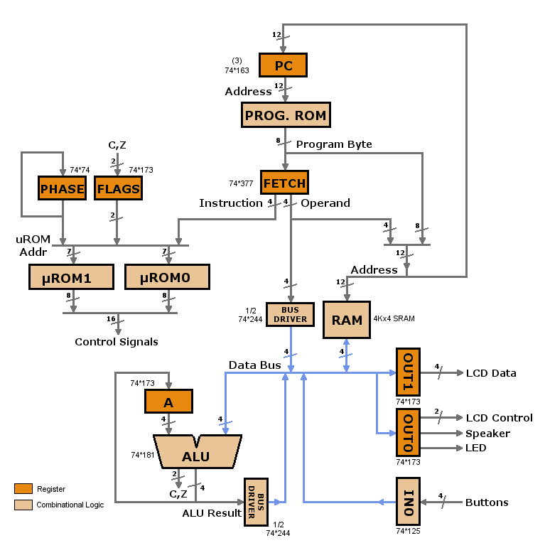
Timing
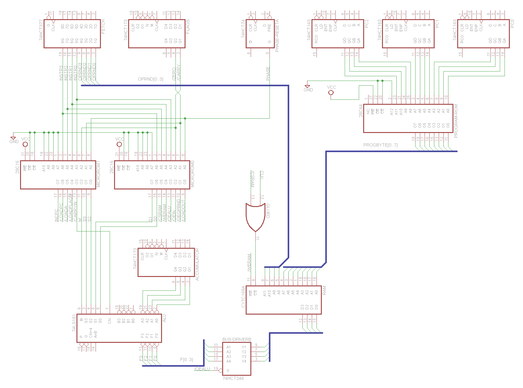
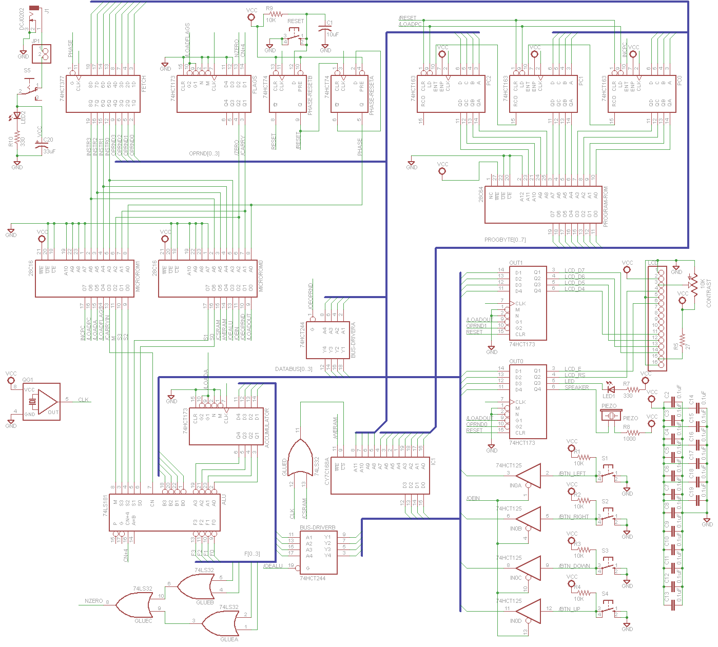
Click on the simplified schematic at the top of this post to see what’s involved while the accumulator value is being written to RAM.
My best guess is that at the end of a RAM write, either the data or the address are changing before the RAM /CS is de-asserted. /CS comes from a 74LS32 OR gate with a max propagation delay of 22 ns. The clock is one of the OR inputs, so /CS will be de-asserted no more than 22 ns after the rising edge of the clock. Could the RAM data or address be changing during this window?
Address: The high address bits come from the Fetch register, whose value never changes at the same time as a RAM write. The low address bits come from the program ROM, which has a 150 ns propagation delay, on top of the PC regsiter’s 39 ns tcq delay, so it seems very unlikely those values could change within 22 ns of a clock edge.
Data: The data is a little more complicated. The value coming from the accumulator won’t change, but the ALU function might, or bus driver B might become disabled, or something else might start driving the data bus and cause contention. All of those would require changing control signals in order to happen. Control signals come from the microcode ROMs, which have a 150 ns propagation delay, on top of tcq delays of about 30 ns for the registers at their inputs. So it seems unlikely the data values could be changing within 22 ns of a clock edge either.
A few other things I tried:
- Replaced the 74HCT244 bus driver with a 74LS244 – This helped a lot, but didn’t completely eliminate the problem.
- Changed TEST_LOCATION to $000 – The test still failed intermittently, but not as much as before
- Changed TEST_LOCATION to $FFF – The test passed reliably
I’m not even 100% certain that the problem is with address or data becoming invalid before the /CS de-assert. Maybe address isn’t valid before the /CS assert, or maybe there’s a glitch on /CS or /WE at some other time. But I don’t think so.
What I really need to do is hook up an oscilloscope or logic analyzer, and look at the relative timing of the clock, /CS, data, and address to see what’s going on. Unfortunately I only have one working scope probe, and even if I had more, I’m not sure the scope has enough resolution to see a timing error of a few nanoseconds. And even if I can demonstrate that data or address are changing before /CS de-assert, I’m not sure what I could do to fix it without major changes. Hmmmm…
Read 27 comments and join the conversationHomemade CPU First Boot
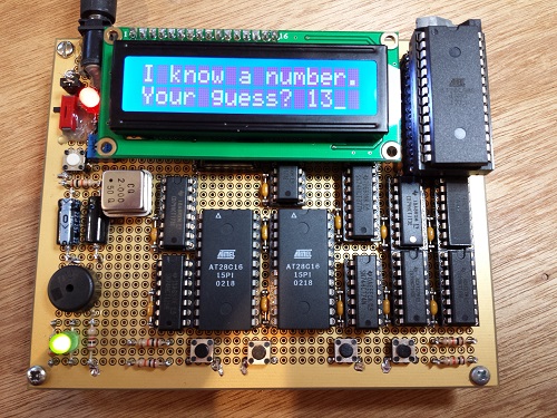
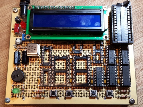
YES, IT WORKS! The Nibbler homemade CPU is up and running, and it can play “guess the number” like nobody’s business. Awesome! If you haven’t seen my earlier posts, Nibbler is a 4 bit CPU built from standard 7400 series logic chips – individual counters, registers, buffers, and gates. It’s an educational example of a simple CPU that’s easy to understand and build, but still capable of running games and other interesting programs. The CPU contains 17 chips in total.
With all the advance design work and simulation that went into Nibbler, I was fairly confident it would work, but it’s sure nice to see it confirmed in real hardware. Construction was slow and tedious, but went fairly smoothly. After soldering the buttons and passive components, the chips were mounted in sockets and connected by wire-wrap. The whole construction process took about five days.
Some specs:
- 4 bit custom-made CPU
- 12 bit addressing, 4K address space size
- Harvard architecture – separate program and data memory spaces
- 2 MHz clock speed, 2 clocks per instruction = 1 million instructions/sec
- Thirteen 7400-series chips in the CPU data and control paths
- Two 28C16 EEPROMs store microcode for generating internal control signals
- 4K x 4 SRAM (CY7C168A)
- 28C64 EEPROM stores programs
- Four pushbutton inputs
- 16 x 2 character LCD
- Audio speaker
- About 100 mA current draw at 5V
For lots more detail on how Nibbler works, see the project home page.
Fun with Debugging
During construction, I ran into a couple of errors in my schematic. I accidentally reversed the Zero and Carry inputs to the microcode ROMs. You’d think that would be an easy thing to catch – notice that all the instructions involving the Carry flag didn’t work, double-check the wiring, and aha! Unfortunately it didn’t happen that way at all.
At the time I ran into this problem, I was part-way through construction, and I hadn’t yet connected the Flags register’s Zero input to anything. It was just floating. Because of my schematic mistake, the CPU was actually using this undefined Zero flag when it thought it was using the Carry flag. The crazy thing was that it still worked sometimes! After powering on the CPU, the Carry flag appeared to work normally and programs ran fine for about two seconds, after which the whole thing went to hell. Because it worked briefly, I assumed there was some kind of overheating problem, or maybe a timing problem caused by changing propagation delays as the chips warmed up. I spent almost a whole day trying to track down the problem. At least it gave me an excuse to use my logic analyzer!
Debugging the Carry flag with the logic analyzer
How is it possible that the CPU worked for a few seconds, when it was using the completely wrong flag? It turns out that because Zero wasn’t yet connected to anything, and the Zero and Carry wires ran side-by-side, capacitive coupling caused the floating Zero input to follow the value of the Carry flag, at least for a little while. What?! Yup, the combination of reversed wires and an unconnected input caused the right value to jump to the wrong wire. After a few seconds, some stray capacitance somewhere charged up to the point where this little trick no longer worked, and the CPU conked out. As soon as I swapped the wires and connected the Zero input properly, the CPU began working nicely.
Son of BMOW 1
It’s interesting to compare Nibbler with BMOW 1, my first homemade CPU. Compared with BMOW 1, Nibbler is tiny! The whole thing fits in the palm of my hand. BMOW 1 looks like a giant in comparison. And Nibbler has just 17 chips, all of which are either memory or 7400 series logic. BMOW 1 has 65 chips, many of which are GALs (programmable logic). The size discrepancy would be even greater if BMOW 1 were constrained to use only 7400 series logic.
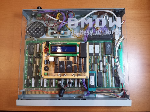
How can Nibbler be that much smaller? The major difference is that BMOW 1 supports lots of I/O devices that Nibbler doesn’t, like a PS/2 keyboard, VGA video, a serial port, 3-voice audio, and a real-time clock. All those device support chips really add up. BMOW 1 also has wider data and address paths, and has a hardware stack register and some other CPU features that Nibbler lacks. BMOW 1 is a very cool machine, but it carries a lot of bloat, making it difficult for people to understand how it all works. Nibbler is more like a minimal CPU example, with just enough power for a few basic games and demos.
Wires!
Because this is the “Big Mess o’ Wires” blog, I’ll conclude with some gratuitous wiring photos. Enjoy!
Read 12 comments and join the conversation
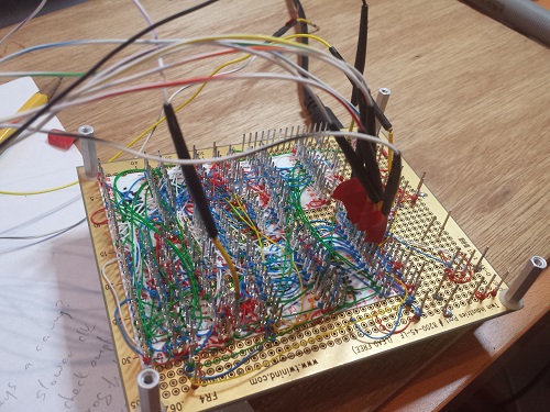
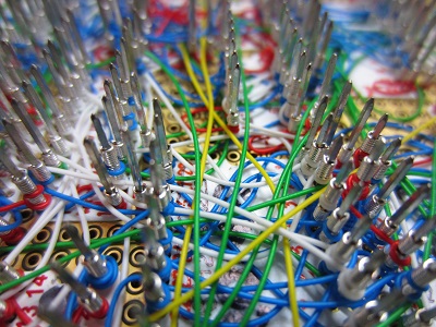
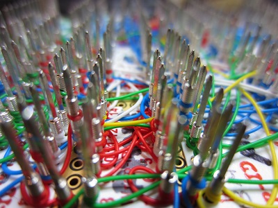
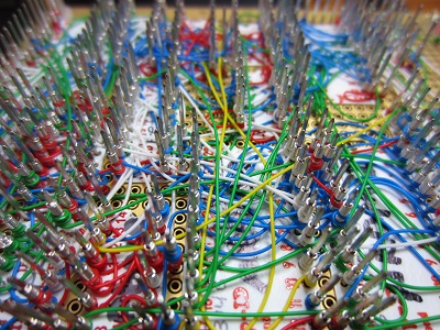
Wire Wrapping the Nibbler CPU
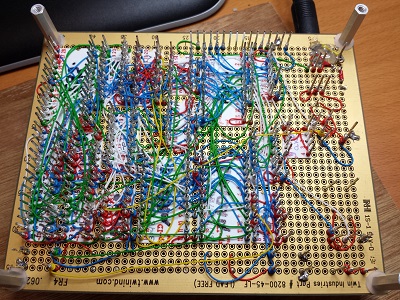
Nibbler construction is underway! I’m building the CPU on a 5 x 4 inch perfboard, and connecting the components using wire wrap. This particular perfboard is a Twin Industries 8200 Series, which has continuous metal planes on both sides that can be used for power and ground. Because the holes don’t go all the way to the edges of the board, the usable area is just 4.5 x 3.5 inches (114 x 89 mm) – about the same size as my mobile phone. It’s very compact. There’s enough extra space for two more 0.3 inch chips, if I later decide to add to the system.
Unfortunately construction didn’t start smoothly. The board didn’t have any mounting holes, and you can see in the photo what a lousy job I did trying to drill four evenly-spaced holes in the corners. After drilling, I made legs by putting screws through the top into 1 inch aluminum standoffs underneath. I quickly discovered that top-side screws in bottom-side standoffs formed an electrical connection, shorting the ground and power planes! Ugh. Inserting nylon washers between the standoffs and the bottom of the board solved that problem, but it wasn’t the last of the challenges.
These kinds of boards are great for mounting and connecting DIP chips, but not so great for anything else like discrete components or buttons. Anything that doesn’t have 0.1 inch spaced pins requires bending or drilling, and discretes also require soldering instead of wire wrap. It took me several hours to drill holes for the DC power jack, deform the button pins to a 0.1 inch spacing, and mount and solder all the other passive components. In many cases that involved cutting a wire so it could be soldered at one end, but wrapped at the other end. What a pain in the butt.
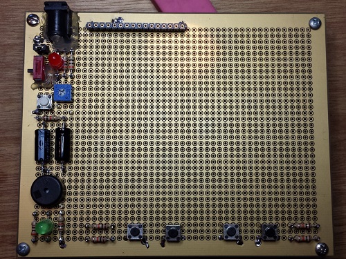
After placement of the discrete components
Soldering anything to this board is surprisingly hard. Each hole is separated from the plane that surrounds it by a circular ring of soldermask. In order to connect a discrete component’s pin to the power or ground planes, the solder must bridge across this ring, and that’s something the solder definitely doesn’t like to do. More and more solder must be added, until it suddenly flows across the ring *and* into the neighboring hole, creating an accidental short. Grrrr! With practice I was able to avoid this, but each solder point was a trial of patience.
After placing all the discrete components, I did a trial fit of all the wire wrap sockets, mounting all the chips inside them. It’s a good thing I did, because there were clearance problems all over the place! If I’d wired up half the system before discovering the clearance issues, I would have been in big trouble. The worst problem was the 74HCT74 for Phase and Reset. Although it’s a 14-pin chip, its package is so elongated, it actually needs more room than other 16-pin chips! I also found a few vertical clearance problems. The LCD is supposed to sit on top of several chips, but I discovered there wasn’t as much space as I’d expected available under the LCD. I’m going to have to build some kind of vertical extension for the LCD, in order to raise it high enough to clear the chips under it.
The last big hurdle was the ZIF socket for the program ROM. I know from past experience that I’ll be swapping that ROM in and out frequently, and I don’t want to have to use a chip puller each time. A ZIF socket will solve the problem, but wire wrap ZIF sockets don’t exist, or are so rare that it amounts to the same thing. I ended up soldering a standard ZIF socket to two rows of machine pin male header, and then inserting the header into a wire wrap socket. It’s not pretty, and the socket sandwich is more than an inch tall, but it works!
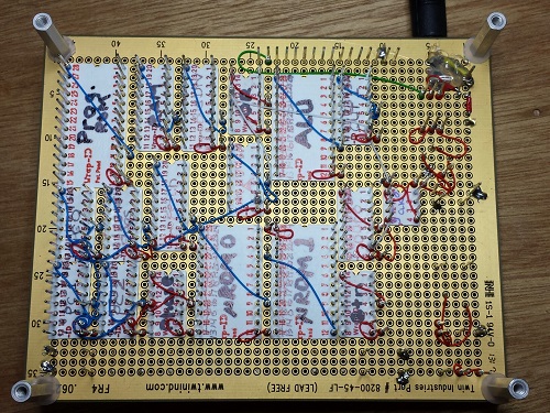
The wiring side, after placement of the power, ground, and clock lines
Nibbler Refinements
I’ve made a few refinements to the Nibbler design, and now I’m ready to start building the CPU! After looking at what seemed like a million different possible changes and additions, I’ve decided to keep the hardware exactly as I originally described it in my first post, with just a few minor changes:
- Replace the ‘175 quad flip-flop with a ’74 dual flip-flop
- Add a ’32 quad OR chip for glue logic
- Replace the ALU’s Equal flag with a Zero flag
- Replace the 2K x 8 RAM with a 4K x 4 RAM
The addition of the OR chip makes the last two changes possible. And although Nibbler will have one more chip than before, I believe it actually makes the overall design simpler to understand.
Flip-Flop: The ‘175 was used for the /RESET signal, and the Phase bit. Because I was only using two of the four FF’s on the ‘175, switching to the smaller package of the ’74 makes sense. The ’74 also has independent clear inputs for each FF, so now /RESET can force Phase to 0, which wasn’t possible with the ‘175.
Zero vs Equal: The original design had an Equal flag, which was set by the ALU’s A=B output as a result of the CMP instruction. This was OK, but a Zero flag is better. It’s set by any instruction that modifies the accumulator, as well as CMP. That makes it possible to do a LD, IN, or NOR, and follow it immediately with a conditional jump JZ or JNZ, without ever doing a CMP. That wasn’t possible with the Equal flag.
The Zero flag is generated by using three OR gates to OR together the 4 bits of the ALU result: /Zero = (F0+F1)+(F2+F3). I considered an alternative method, where the ALU is operated in active low mode, and the operands and output treat a low voltage as logical 1 and a high voltage as logical 0. This makes the ALU’s A=B output behave like a true Zero flag, but requires the use of some inverting buffers, and requires some staring at the datapath diagram and the datasheet before it’s clear why it works. The OR method is much more intuitive.
4-Bit RAM: My original plan called for an 8-bit RAM, with four of the data pins unused. That’s a little awkward, but because none of the 4-bit RAMs I found had a /OE output enable, they couldn’t be used with Nibbler as-is. 8-bit RAMs typically have a /OE pin, making them easier to work with. The reason is somewhat complicated. With only /CE and R/_W inputs on the 4-bit RAM, it’s not possible to enable it for appropriate instructions and gate the write-enable signal with the clock (necessary to prevent accidental writes) without external glue logic.
With the addition of the ’32 quad OR chip, I can use one OR gate for the necessary glue. The /CERAM control signal is OR’d with the clock, and connected to the RAM’s /CE input. This ensures that RAM is only enabled during the second half of the clock cycle, and only during clock cycles where the microcode wants it enabled. The /WERAM control signal is connected directly to the RAM’s R/_W input. If it’s enabled and it’s not writing, then the RAM functions in read mode, and drives a nibble onto the data bus.
New Instructions
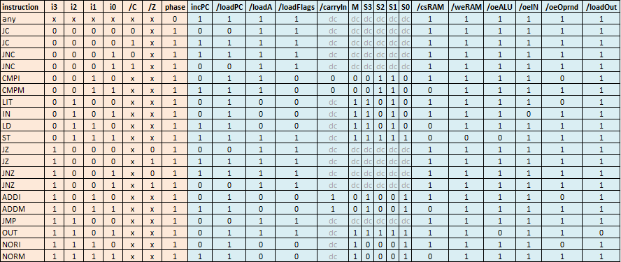
What about possible new instructions? I’ve decided to keep things as simple as possible, and stick to 16 instructions, selected by the high 4 bits of a byte of program memory. Furthermore, I’m only going to consider instructions that can work with the current datapath and control path, and can be implemented solely by changing the microcode ROM contents. That rules out many of the possible new instructions that I discussed previously, but keeps everything much simpler.
So, exactly which 16 instructions will it be? I’m not sure yet, but I don’t have to be. I can update the contents of the microcode ROM after the CPU is built, based on my experience writing programs for it, to select the 16 instructions that prove to be most useful. However, 14 of those 16 are almost certain. The only real question is whether JNZ and JNC should be replaced with something else.
Incidentally, I never realized the double-entendre in “driving the data bus” until now. Maybe when I retire, I’ll buy an old yellow school bus, paint DATA BUS on the sides, and drive it to electronics shows shouting out the window “Look, I’m driving the data bus!” Fun times, guaranteed.
Read 11 comments and join the conversation
Guess the Number
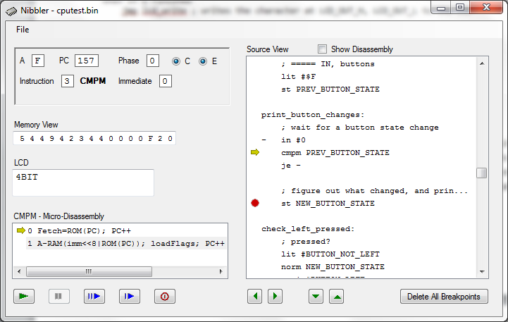
It’s programming time! To verify that Nibbler’s design and instruction set are powerful enough to handle a real program, I sat down to write a simple “guess the number” game. And… (drumroll) it works! I ran the program on the Nibbler simulator, and interacted with it using the simulated pushbuttons. Hint for competitive players: you can always guess the number in at most log2(range) guesses. 🙂
At startup, the program asks the player to press any button. While it waits, it constantly increments a 4-bit counter, incrementing from 0 to 15 and rolling over back to 0. The value of the counter when the player presses the first button determines the secret number he’ll be trying to guess.
Next, the program prompts the player to enter a guess. Pressing the up/down buttons increases/decreases the guess number, and pressing the right button submits the guess. The guess number is converted to text using a crude nibble-to-ASCII conversion routine, which does a byte-wide addition of the number to the character literal ‘0’, performing carry propagation from the low to the high nibble. After submitting a guess, the LCD display changes to “Too high!”, “Too low!”, or “You got it!”, and the player is prompted for a new guess. View the Guess the Number program listing.
While the program runs perfectly on the simulator, there are a few details that probably need to change to make it work on real hardware. Button debouncing code needs to be added, since real buttons don’t cleanly change between their 0 and 1 states, but bounce rapidly between states for a few milliseconds when the button is pressed or released. The LCD initialization and timing code may also be off – I’ll need to verify that on real hardware to be sure.
Program Analysis
The guess the number program assembles to 1135 bytes, or 27% of Nibbler’s program memory. Writing the program was an interesting exercise in coping with the limitations of the CPU’s simple design:
- Registers – Nibbler has just one CPU register: the 4 bit accumulator “A”. Surprisingly, working with only one register didn’t cause many problems, and there were few instances where additional registers would have made a difference.
- Call/Return – The lack of a stack in Nibbler means there’s no call/return mechanism, so no way to call subroutines in the traditional way. This was an annoyance, but I was able to work around it by using a dedicated memory location called
RETURN_ADDRESS, and testing its value at the end of subroutines in order to determine where to jump next.
- Indirect Addressing – All Nibbler memory references use absolute addressing, with no indirect or indexed address modes. This was a bigger annoyance, and working around it led to some ugly code bloat. To get the Nth element from an array of size K, the code must perform K tests of the value of N to determine the correct absolute address. This approach would be impractical in a system using large data structures, but for the types of programs planned for Nibbler, it works OK.
- Program Literals – The biggest headache turned out to be working with arrays of constant data: the character strings like “Press any button”. These had to be copied to data memory one nibble at a time, using LIT and ST instructions, resulting in major code bloat. With this technique, each nibble of constant data requires three bytes of program space. With 4096 bytes of total space, this limits Nibbler programs to a few hundred bytes of strings and other constant data, but that should be enough.
Tool Updates
Along the way, I made a few improvements to the toolchain. The Nibbler assembler gained the ability to do basic math on address labels, such as
ld LCD_BUFFER+1
to load the accumulator from the second nibble of LCD_BUFFER. This proved to be extremely useful, as you can see in the program listing.
The second major improvement was to the simulator. I grew curious how fast the simulation was running in comparison to the planned clock speed of the real hardware, so I added a simulated MHz status line at the bottom of the simulator window. It turns out that the simulation runs faster than the real thing, averaging about 3 MHz when running on a 2.5 GHz Core i5 computer. Not bad for managed .NET code that was written with no thoughts for performance optimization.
Read 17 comments and join the conversation
Nibbler Software Tools
During development of the Nibbler CPU, I’ve created several software tools to help make my life easier. Some of these have been nearly as interesting as the CPU itself! While professionally I work with C++ or Java, for my personal projects I find the .NET languages like C# to be most convenient. They include a robust set of libraries for common data structures and I/O, and also make it a snap to build a GUI. To create my tools I use the free Visual Studio Express IDE, running on Windows. There are plenty of other development options like Eclipse and the GNU tools, but I’m already familiar with the Visual Studio IDE, and the $0.00 price is hard to beat!
Microcode Assembler
The simplest tool is the Microcode Assembler, which doesn’t actually assemble anything, but instead generates two binary files for the contents of the two microcode ROMs. The program is written in the version of C++ that uses managed code and the .NET foundation. I’ve never been entirely clear what the proper name for it is: Managed C++, or Visual C++, or C++/CLI?
In the beginning I intended to describe the microcode operations in a text file, using register transfer language, and then the Microcode Assembler would assemble it into binary. But when it became clear the microcode would be fairly simple, I dropped the idea of using RTL, and just wrote some C++ code to directly generate the required binary data. Using the microcode table from my previous post, this was a quick task. The program contains lots of bit-shifting fun like:
    // 9 JNE
    for (int c = 0; c < 2; c++)
    {
        microcode[(9 << 3) | (c << 2) | (0 << 1) | 1] = 0x383F; // NE
        microcode[(9 << 3) | (c << 2) | (1 << 1) | 1] = 0xF83F; // E
    }
Whee! Those hexadecimal numbers are just rows from the microcode table, with the 16 control signals expressed as a 4-nibble hex value. Nothing very exciting here, but it gets the job done.
Assembler
I needed some way to write programs for the CPU, using symbolic instruction names and branch labels, instead of stringing together opcode values by hand. Woz supposedly hand-assembled most of the Apple II ROM routines, which is damn impressive, but not really something I wanted to duplicate.
I considered taking an existing open source assembler and modifying it for my needs, but as it turned out, I already had a suitable assembler that I’d previously written for my Tiny CPU project. With a few hours of work, I was able to adapt that assembler for Nibbler’s purposes.
Unlike the other tools, the assembler is written in vanilla C++, and runs as a command line program. It takes a single .asm file as input, and assembles the code into a .bin binary output file. It also generates a .sym symbol file, containing the values of all the labels and constants in the code, as well as the assembled address of each line of code. The symbol file is used later by the simulator, in order to perform source-level debugging.
The assembler doesn’t have any fancy features like macros or conditional compilation, but it does support:
- Decimal constants
- Hex constants, preceded by $
- Character constants, contained in ‘ ‘ single quotes
- < and > operators to extract the high or low nibble of a byte constant
- Named constants using #define (both data and address constants)
- Named labels, and jumping to a named label
- Unnamed + and – labels, for jumping forward and backward
- Comments, starting with ;
Here’s a snippet from an example .asm file, showing the kind of code the assembler can handle. This snippet watches the input buttons, and writes a character to the LCD whenever a button transition occurs.
    ; example.asm

    ; memory locations
    #define PREV_BUTTON_STATE $00D
    #define NEW_BUTTON_STATE $00C
    #define RETURN $00F
    #define LCD_OUT_H $000
    #define LCD_OUT_L $001

    ; buttons
    #define BUTTON_LEFT $1
    #define BUTTON_NOT_LEFT $E

    begin:
        ; reset the button state
        lit #$F
        st PREV_BUTTON_STATE

    print_button_changes:
        ; wait for a button state change
        -   in #0
        cmpm PREV_BUTTON_STATE
        je -

        ; save the new state, and determine what changed
        st NEW_BUTTON_STATE

    check_left_pressed:
        ; is left button currently pressed?
        lit #BUTTON_NOT_LEFT
        norm NEW_BUTTON_STATE
        cmpi #BUTTON_LEFT
        jne check_left_released

        ; was it previously unpressed?
        lit #BUTTON_NOT_LEFT
        norm PREV_BUTTON_STATE
        cmpi #BUTTON_LEFT
        je check_right_pressed

        ; left button changed from unpressed to pressed: print an upper-case letter L
        lit #<'L'
        st LCD_OUT_H
        lit #>'L'
        st LCD_OUT_L
        jmp print_button_change

    check_left_released:
        ; was left button previously pressed?
        lit #BUTTON_NOT_LEFT
        norm PREV_BUTTON_STATE
        cmpi #BUTTON_LEFT
        jne check_right_pressed

        ; left button changed from pressed to unpressed: print a lower-case letter L
        lit #<'l'
        st LCD_OUT_H
        lit #>'l'
        st LCD_OUT_L
        jmp print_button_change

    check_right_pressed:
        ; ...handle the other buttons

    print_button_change:
        lit #1
        st RETURN ; store 1 at RETURN, lcd_write uses this to know it should jump to next1 when it's finished
        jmp lcd_write ; writes the character at LCD_OUT_H, LCD_OUT_L to the LCD

    next1:
        ; update the previous button state to the new state
        ld NEW_BUTTON_STATE
        st PREV_BUTTON_STATE
        jmp print_button_changes
Simulator
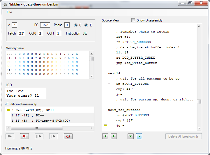
The most complex tool by far is the machine simulator. Originally developed for BMOW, this GUI-based tool is written in Managed C++, and simulates the data and control paths of the CPU. It supports source level symbolic debugging, disassembly, microcode debugging, code breakpoints, data breakpoints, memory inspection, and I/O simulation of the LCD and input buttons. It’s not perfect, but it’s a sweet tool that makes diagnosing problems dramatically easier than it would be otherwise. And who doesn’t love simulation?
The simulator uses the assembled program binary, the program source and symbol files (if available), and the microcode ROM binaries. Because it uses the microcode to control the data paths, it needs no special knowledge of Nibbler’s instruction set in order to do the simulation: it’s just a dumb series of paths governed by control signals, same as the real hardware. But for the sake of code disassembly and debugging, there is some knowledge of the Nibbler instruction set built in.
In the image above, the simulator is doing source level debugging of a program similar to the previous button watcher example. Execution is currently stopped at the CMPM PREV_BUTTON_STATE instruction, as shown by the yellow arrow. There’s a breakpoint two instructions further down, at the line with the red circle. If the simulator is started and a sim-button is pressed, the program will break out of the loop and stop at the breakpoint. Yahoo, interactive debugging!
From right to left, the simulator control buttons are:
- Run – Keep simulating until explicitly paused, or a breakpoint is hit
- Pause – Momentarily stop the simulation
- Microstep – Simulate one clock cycle, then pause
- Step – Simulate to the start of the next instruction, then pause
- Reset – Set the program counter to 0
The upper-left shows the current CPU state, and the contents of RAM. Below those is a 16×2 character LCD display, using a partial simulation of the LCD’s HD44780 controller module driven by the OUT0 and OUT1 ports.
At the bottom left is a microcode “disassembly” of the current instruction. In this case for the instruction CMPM, phase 0 uses the PC as an address into ROM, retrieving a byte which is stored in the Fetch register. Phase 0 also increments the PC. Phase 1 uses the ALU to calculate A minus RAM(addr), where the RAM address is formed from the immediate opcode value and the current program ROM byte, as described in previous posts. It also loads the C and E flag registers with the result of the ALU calculation, and increments the PC.
For all its capabilities, the simulator won’t catch every problem that might occur on the real hardware. It’s purely a dataflow simulator, and has no concept of timing at a finer resolution than one clock cycle. If there’s a race condition somewhere, or a timing requirement that isn’t met, the simulator won’t detect the problem. It’s also too forgiving of microcode errors that would break the real hardware, like enabling multiple sources to drive the data bus as the same time. But despite these shortcomings, I’ve found the simulator to be an incredibly helpful tool. And it’s a huge confidence boost to see everything running in the simulator, before building the actual hardware. 🙂
Read 3 comments and join the conversation