

Archive for the 'Tranz 330' Category
Tranz 330 Files
 I’ve posted an archive containing the original Tranz 330 program file dump, my commented disassembly of the original program, and two versions of the Mozart demo in source and binary form. If you can get your hands on a Tranz 330 from a surplus electronics supplier, this should give you an afternoon’s entertainment! You can grab the files here.
Mapping the Tranz 330
 The VeriFone Tranz 330 point of sale terminal and its cousins are great platforms for electronics tinkerers. Commonly available from surplus stores or eBay for around $10, these little boxes contain a complete 8-bit computer, with lots of intersting I/O interfaces and a retro-styled vacuum-fluorescent display. The Tranz uses the Z-80 microprocessor, same as the venerable TRS-80 and ZX Spectrum, so software routines from those classic computers can often be reused.
The default program in the terminal’s ROM is a rather dull credit card processing application, but a new program can be substituted by replacing the original ROM chip. With knowledge of the hardware and a Z-80 assembler, you can write a new program to make the Tranz do any crazy thing you can imagine, like Mozart’s Credit Card: turning credit card magnetric stripe data into music. This guide will show you how.
Systems Specs
- Z-80 CPU at 4 MHz
- 32K ROM, in a socket for easy replacement
- 32K RAM
- 16 character, 16 segment vacuum fluorescent alphanumeric display
- 16 key 4×4 keypad
- Piezo speaker
- Magnetic stripe card reader, ISO 7813 Track 2 format
- Z-80 PIO, parallel port interface
- Z-80 DART, serial port interface
- Z-80 CTC, counter/timer
- OKI M6242B Real-time calendar/clock chip
- Micrel MIC10937 display controller
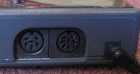
- RS-232 serial port, 8-pin DIN connector
- Accessory serial port, 6-pin DIN connector
- 73K212L-IP single chip 1200 bps modem
- Internal lithium battery backup for RAM
Related Tranz Terminals
VeriFone also produced several similar Tranz terminal models. I haven’t used these, but most of what’s written here about the Tranz 330 should also apply to them. Software written for the Tranz 330 may need small modifications to account for hardware differences on these other terminals, however.
- Tranz 380 – Z180 CPU at 6 MHz, 64K ROM, 64K or 128K RAM, track 1/2/3 card reader
- Tranz 460 – Z80A at 3.579 MHz, track 1/2 card reader, integrated receipt printer
Power Requirements
Used Tranz 330 terminals are often sold cheaply without the AC adapter, but fortunately replacements are inexpensive. The important thing to be aware of is that it requires an AC-to-AC adapter, not AC-to-DC. The stock VeriFone adapter outputs 8.5VAC at 1 amp. I have also successfully used Jameco part number 1586154, which is a 9VAC 1 amp adapter for $7.95. Any other similar adapter with a 2.5mm inner diameter should also work.
Why does the Tranz 330 use an AC-to-AC adapter instead of AC-to-DC? I don’t know, and I didn’t investigate. On-board power regulation is provided by an L387A low dropout 5V DC regulator, and all of the digital electronics use a 5V DC supply. Maybe this was a cost-saving measure of some kind?
I/O Board Interface
 Inside the Tranz 330 case, the components are split between two circuit boards, stacked on top of each other and joined only by a single 20-pin 0.1 inch connector. The logic board is on the bottom, and contains the CPU, support chips, power supply, serial ports, and modem. The I/O board is on the top, and contains the keypad, display, MIC10937 display controller, and speaker.
For people using a microcontroller instead of the Z-80, the logic board can be discarded, and the I/O board and case used alone. The connection between the boards is not soldered, so they can be easily separated. This makes a nice self-contained I/O solution for a microcontroller project, with all the necessarily signals available at the 20-pin header.
I/O Board Connector Pinout
- keypad top row
- keypad second row from top
- keypad third row from top
- keypad bottom row
- keypad right-most column
- keypad second column from right
- keypad third column from right
- keypad left-most column
- NC
- NC
- NC
- card reader output
- display reset
- display data input
- display clock
- +5V DC
- speaker driver input
- -5V DC
- speaker mute?
- GND
Note pin 17 is actually connected to the clock input of a flip-flop in the speaker driver, and not directly to the speaker itself, and so the I/O board is only capable of playing square waves of various frequencies. Pin 19 is connected to the FF’s asynchronous set input. Pin 12 is the signal from the card magnetic read head, and must be decoded as described below in the section about the card reader.
Making a Replacement ROM
 If you keep the logic board, you’ll need to replace the original ROM with one containing your new program. The original ROM is a 28-pin, 32K (256 kbit) 27C256 UV-erasable EPROM. Assuming you don’t already own a UV eraser and enjoy spending 15 minutes erasing your EPROM each time you change your program, you’ll want to replace this with a more modern 32K EEPROM or Flash ROM.
You’ll need an EPROM/EEPROM/Flash universal programmer to make your new ROM. If you don’t already have one, MCUmall has a good selection of inexpensive programmers. I use the EasyPro 90B.
Unfortunately no currently-manufactured EEPROM or Flash exactly matches the capacity, physical size, and pinout of the 27C256. The best solution is to use a 27SF512 Flash ROM. This is a 64K ROM, but if you place your program in the upper half (configure your programmer’s software to place the data at $8000), it is pin-for-pin compatible without any further work needed. Sadly, the 27SF512 is no longer manufactured, but is still commonly available from secondary sources and auto parts suppliers, since it’s a favorite of people who re-chip their car’s electronic fuel injection controller.
An alternative solution using all-new parts is to use a 28C256 EEPROM. This is a 32K ROM, but the pinout is slightly different than the 27C256. To make it work, after burning the ROM, pin 27 should be bent up and soldered to pin 28. Make sure that pin 27 does not contact the socket. Of course, this makes it impossible to reprogram the ROM later, so you may want to do this modification to a low-profile ZIF socket instead of the 28C256 itself. As before, you also must place your program in the upper half of the ROM (configure your programmer’s software to place the data at $4000). Since the 28C256 is a 32K device, this limits you to a total ROM image size of 16K. I used this method successfully until I found a supply of 27SF512 chips, but it can be difficult to get a reliable electrical contact between the ZIF and the underlying ROM socket.
Software Tools
Your program will be written in Z-80 assembly language, so you’ll need an assembler. I used sjasm, but any Z-80 assembler will work. You may also want a Z-80 simulator to help test your code before burning it to ROM. I used an evaluation version of Z80 Simulator IDE.
You may find some online references to “programming” the Tranz 330 in a propriety language called TCL. Ignore these. TCL is an ugly run-time interpreted language for making custom point of sale applications, and the interpreter is part of the original ROM. TCL programs run inside the sandbox provided by the interpreter. You’ll be making a native Z-80 program that has direct access to all the hardware.
Tranz 330 Library Routines
 While creating the Mozart’s Credit Card demo, I developed a set of reusable library routines for working with the Tranz 330 hardware. These routines simplify common tasks like printing a string to the display, reading the keypad, and playing a tone on the speaker. The file tranz330.asm contains all these library routines, as well as the Mozart demo program to serve as a working example. Use this as a starting point for making your own Tranz 330 programs. Portions of the library routines also appear below in the hardware-specific sections.
You can also download an archive containing the original Tranz 330 program file dump, my commented disassembly of the original program, and two versions of the Mozart demo in source and binary form.
Tranz 330 library routines Tranz 330 + Mozart archive
Memory Map
The Z-80 has a 64K memory address space. ROM is mapped to addresses 0 – $7FFF. At startup, program execution begins at address 0. RAM is mapped to addresses $8000 – $FFFF. Typically the stack will begin at $FFFF, growing downward.
I/O Ports
The Z-80 also has a separate 256 port I/O space. For the Tranz 330, these ports are mapped as follows (all port numbers in hex):
- Port $00 – PIO parallel port A.
- Bits 3-0: output, keypad columns. Bit 3 is right-most column.
- Bit 4: output, display controller reset
- Bit 5: output, display controller data
- Bit 6: output, display controller clock
- Bit 7: input, card reader data
- Port $01 – PIO control register for port A.
- Port $02 – PIO parallel port B.
- Bits 3-0: input, keypad rows. Bit 3 is bottom row.
- Bits 7-4: not connected
- Port $03 – PIO control register for port B.
- Port $10 – CTC channel 0
- Port $11 – CTC channel 1
- Port $12 – CTC channel 2. Chan 2 output is connected to speaker driver.
- Port $13 – CTC channel 3. Chan 3 input trigger is connected to chan 2 output.
- Port $20 – DART serial port A. 8-pin DIN RS-232 port.
- Port $21 – DART control register for port A.
- Port $22 – DART serial port B. 6-pin DIN accessory port.
- Port $23 – DART control register for port B.
- Ports $30 – $3F – Real-time clock registers $0-$F
- Ports $40,$50,$60,$70 – Modem?
Most applications will use the PIO parallel ports. Complete details on using the PIO can be found in the Z-80 PIO user’s manual. For the Tranz 330, this library routine will initialize the ports with the necessary settings:
system_init:

LD A,0xCF           ; control each port bit individually

OUT (0x01),A

LD A,0x80           ; bit 7 is input, others are outputs

OUT (0x01),A

LD A,0x18           ; use interrupt vector 18

OUT (0x01),A

LD A,0x97           ; generate interrupt if any masked bit is low

OUT (0x01),A

LD A,0x7F           ; interrupt mask = bit 7

OUT (0x01),A

LD A,0x3F           ; set the initial output values for port 0

OUT (0x00),A

RET
Display
![]() The 16-character, 16-segment VFD is powered by a Micrel 10937 display controller. It supports upper-case letters, digits 0-9, and a small selection of symbols.
The 16-character, 16-segment VFD is powered by a Micrel 10937 display controller. It supports upper-case letters, digits 0-9, and a small selection of symbols.
The controller is connected to the CPU through a serial interface, using port $0 bits 6-4. Data bytes must be shifted in to the controller one bit at a time. The serial clock must also be toggled via software for each bit. Data bytes are 8 bits, and are transmitted MSB first. An MSB of 1 indicates a control byte, and an MSB of 0 indicates a data byte to be displayed.
After a reset, the display is turned off by default. Before printing anything, it must first be turned on by setting the display duty cycle to something higher than zero.
display_init:

IN A,(0x00)         ; get current port state

AND 0xEF            ; clear bit 4 (display reset)

OUT (0x00),A

LD B,0x1C           ; wait 0x1C cycles

.L1 DJNZ .L1

OR 0x10             ; set bit 4 (display reset)

OUT (0x00),A

LD C,0xFF           ; set the display duty cycle to 31 (maximum brightness)

CALL display_send_byte

RET
Sending a control or data byte to the display requires shifting it out one bit at a time on port $0 bit 5, while toggling the serial clock on port $0 bit 6:
display_send_byte:

; byte to be sent is in C

; note the display controller does not support lower-case letters!

LD B,0x08           ; 8 bits to send

.L1 IN A,(0x00)         ; get current port state

RLA                 ; rotate the port word until the data bit is in the carry flag

RLA

RLA

RL C                ; shift the next output data bit into the carry flag

RRA                 ; rotate the port word until the data bit is in bit 5

RRA

RRA

OUT (0x00),A        ; setup the data output (bit 5)

OR 0x40             ; set clock high (bit 6)

OUT (0x00),A

AND 0xBF            ; set clock low (bit 6)

OUT (0x00),A

DJNZ .L1            ; continue with the next bit

RET
Keypad
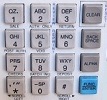 The 16-key keypad is arranged in a 4×4 layout. It contains a 12-key telephone-style section with the digits 0-9, *, and #, as well as the four special function keys CLEAR, BACKSPACE, ALPHA, and ENTER. The keypad is a passive device, requiring work from the CPU to test the keypad state. The keypad has four column lines and four row lines, and the row lines have pull-up resistors. When a key is pressed, an electrical connection is made between the row and column lines that overlap beneath that key.
By driving a 0 to a single column line while driving a 1 to the others, the CPU can activate that column. The current state of the four keys in that column can then be tested by reading the row lines. If a key in an active column is pressed, the corresponding row line value will be 0. If no key is pressed, the pull-up resistor will supply a value of 1 for that row. To detect key presses, the CPU must activate each of the four column lines in turn, and check the row lines for 0’s.
The column lines are connected to the CPU on port $0 bits 3-0, and the row lines on port $2 bits 3-0.
The library function keypad_read returns a key code in the range 1-16 in A, or 0 if no key is pressed.
To enter a multi-character string involving letters, numbers, and symbols, a higher-level input routine is needed. The library function keypad_get_string reads a complete string from the user, and provides some basic line editing capabilities. Key presses are echoed to the display. BACKSPACE can be used to correct mistakes. Letters and special characters can be entered by first pressing a number key, and then repeatedly pressing ALPHA to cycle through the alternate characters for that key. String entry concludes when ENTER is pressed.
CTC and Speaker
The Z-80 CTC has four independent counter/timer channels, addressable by the CPU on ports $10 – $13. Complete details on using the CTC can be found in the Z-80 CTC User’s Manual. The channels can be configured to trigger an interrupt when timeout occurs. Each channel also has a timeout pin and a trigger pin for direct hardware interfaces. On the Tranz 330, the channel 2 timeout pin is connected to the clock input of a flip-flop in the speaker driver, and also to the channel 3 trigger.
A square wave tone of any desired frequency can be played through the speaker by setting an appropriate time constant on channel 2. Unfortunately, there’s no way to control the volume or create other audio waveforms.
To configure channel 2 for speaker usage, it must be set to timer mode with auto-triggering. The desired frequency can then be played by loading an appropriate time constant into channel 2:
speaker_beep_period:

; beep tone period time constant should be passed in C

LD A,0x07           ; disable interrupts, timer mode, prescale=16, auto-trigger, time constant follows

OUT (0x12),A

LD A,C              ; time const

OUT (0x12),A        ; speaker on

LD BC,0x0096       ; wait 150 ms

CALL wait_ms

LD A,0x03

OUT (0x12),A        ; speaker off

RET
Card Reader
The card reader supports ISO 7813 Track 2 format, which is up to 40 characters, where each character is 4 data bits and one odd parity bit. It will read virtually any credit card, driver’s license, shopping card, ID card, or other card with a magnetic stripe. Typically the data on the magnetic stripe is the same as what’s printed on the card: account number and expiration date. In many cases, depending on the type of card, some additional data may be stored as well. The magnetic stripe does not contain PINs or other private data.
The card reader is connected to the CPU on port $0 bit 7. The port is configured to trigger an interrupt whenever the card reader signal is active. At the CPU interface, the card reader signal is normally 1 when no card is present, and toggles rapidly between 1 and 0 when a card is swiped. If you’re using the I/O board with a microcontroller and directly sensing pin 12 from the 20-pin header, then the polarity is reversed: the signal is normally 0, and toggles rapidly between 1 and 0 when a card is swiped.
Interpreting the card reader signal is complex, because there is no clock signal, the speed at which the data signal changes depends on the speed the card is swiped, and because the signal doesn’t even directly provide the logical binary data from the card.
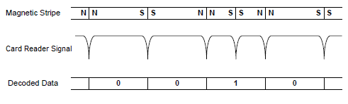 A track on the magnetic stripe consists a long series of magnetic domains. Each domain is polarized magnetic North or South. When the read head is over a domain of either polarity, the card reader signal is 1. When the read had passes over the boundary between domains of opposing polarities, the card reader signal briefly pulses to 0. The duration of this pulse is approximately 40 microseconds.
Each logical data bit on a track has the same physical length on the magnetic stripe. There will always be a magnetic domain boundary at edge of a bit. A logical 1 bit will also have a magnetic domain boundary within the length of the bit, but a logical 0 will not. Extracting logical 0’s and 1’s is therefore a task of measuring the intervals between pulses of the card reader signal. Two successive pulses each time N since the last represent a logical 1, and a single pulse time 2N since the last represents a logical 0. This encoding format is called F2F or Aiken Biphase.
The data begins with a long string of logical 0’s, enabling the software to calibrate the value of N for that swipe of the card. For better reliability, the card reader library routine also adjusts the value of N during bit transcription, to compensate for an accelerating or decelerating motion during the card swipe.
Using the library routines for the card reader is a multi-step process:
- At startup, system_init sets the interrupt handler to be called when the card reader signal pulses low.
- The interrupt handler uses a busy loop to measure the duration of each 0 to 1 cycle of the card reader signal, storing the duration data in a buffer. When the handler terminates, control is returned to the routine got_card.
- card_parse_bits is called to perform the F2F decoding of the duration measurements, filling the buffer with logical 0’s and 1’s.
- card_parse_characters is called to convert the logical bits into ASCII characters, filling the buffer with a null-terminated ASCII string. The ASCII conversion adds $30 (ASCII ‘0’) to each 4-bit datum. If a parity error is detected, the empty string is returned.
The final string returned will begin with a start sentinel (ASCII ‘;’), contain up to 40 characters of content, and end with an end sentinel (ASCII ‘?’). The data content typically begins with the account number (up to 16 characters), followed by a ‘=’ field separator, expiration date in YYMM format, and finally other data specific to the card provider.
Serial Ports
 The Tranz 330 has two serial ports: an RS-232 port with 8-pin DIN connector, and an accessory serial port with 6-pin DIN connector. The serial ports are controlled by the Z-80 DART, which is basically a Z-80 SIO/0 without the synchronous clocking capability. Complete details on using the DART can be found in the Z-80 SIO User’s Manual.
The serial ports are connected to the CPU via the DART on ports $20 and $22. Port $21 is the control register for port $20, and port $23 is the control register for port $22.
I didn’t experiment with the serial ports or write any library routines for them, so people wishing to use the serial ports will need to consult the SIO User’s Manual and write the code themselves. Usage is fairly straightforward: write to port $21 to set the serial port direction and speed, then read/write data from/to port $20.
Real-Time Clock/Calendar
The OKI M6242B real-time clock provides a mechanism to query and update the second, minute, hour, day, month, and year. Because the Tranz 330 has an internal backup battery, the date and time is retained even when external power is lost. The M6242B has 16 control registers, which are mapped to CPU I/O ports $30 – $3F. Complete details on using the RTC can be found in the M6242B datasheet.
Internal Modem
The 73K212L-IP single-chip modem provides a 1200 bps interface for communication over dial-up phone lines.
I didn’t experiment with the modem or write any library routines for it. From examination of the original Tranz 330 ROM program, I believe the modem is connected to the CPU on one or more of I/O ports $40, $50, $60, and $70. Complete details on using the modem can be found in the 73K212L datasheet.
Feedback
If you find this technical information useful, and make a cool project based on the Tranz 330, please leave a note in the comments!
Errata
The following information was contributed by John Barthol.
The port addresses are correct in your documentation but the SIOA port is mapped to some pins on the modem chip (not the 8 pin DIN). I found that the 8 pin DIN was mapped to SIOB. The pin pad (6 pin DIN) port is mapped to SYNCB on the SIO and one of the pins on the PIO. The system clock speed is 7159090 so the CTC trigger clock is 1/4 of that or 1789772.5. Baud rate can be calculated by BAUD = 1789772.5 / (CTC_TIME_CONSTANT * DART_SCALE_FACTOR). I ended up using a time constant of 186 and scale factor of 1 to get me to 9600 baud. Actual baud is 9622 but it seems close enough.
Read 15 comments and join the conversationMozart’s Credit Card
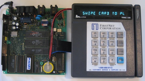 Not long ago, I picked up an old point-of-sale terminal at an electronics surplus store. After discovering a cool little Z-80 based computer inside, and reverse-engineering the hardware, I decided to reprogram it to unlock the music hidden inside magnetic stripe cards. I call this wonder Mozart’s Credit Card.
The hardware is a Tranz 330 POS terminal from VeriFone, dating from the 1980’s. The 330 and its cousins are great for electronics tinkerers. They’re self-contained 8-bit computers with lots of intersting I/O interfaces, and retro-style vacuum-fluorescent displays. They use the same microprocessor as the TRS-80 and ZX Spectrum, so handy software routines from those computers can be reused. The terminals are commonly available from surplus stores or eBay for around $10.
Documentation for the 330 is readily available online, but it only addresses how to use the POS features, with very little hardware information. The Z-80, its support chips, and the other components like the display driver and real-time clock are all well-documented, but to use them, it was necessary to reverse-engineer the terminal’s hardware design. I needed to know how the I/O interfaces were mapped into the address space, which chips were connected to which port pins, and what timing and communication protocol requirements existed. Through a combination of tracking the signal traces by “beeping out” the board, and examining the disassembly of the POS software in the terminal’s ROM, I was able to learn what I needed. I’ll be posting lots more techincal data about the Tranz 330 soon in a separate post, so anyone with one of these little wonder-boxes can reprogram them for creative new purposes.
After due consideration (and a couple of beers), I decided to make a demo that reads data from magnetic stripe cards, and uses it to play music. What song does your Visa play? How about your driver’s license? Ooh, that library card’s got a nice rhythm. Check the video to see Mozart’s Credit Card in action:
Mozart’s Credit Card is a custom program written in Z-80 assembly language. I burned the program to a Flash ROM, and swapped the new ROM for the terminal’s original ROM. Fortunately the 330’s ROM is in a socket, making replacement easy. When a card is swiped, the card reader returns the ISO 7813 Track 2 data, which is up to 40 BCD characters, with 4 data bits and 1 parity bit per character. The raw data uses F2F encoding, in which all bit intervals are the same duration, but a logical 1 has a low-to-high or high-to-low transition during the bit interval, and a logical 0 has the same polarity during the whole bit interval. This F2F signal must be converted into binary data in software.
Once the card data has been read, a rule-based system is used to turn it into semi-acceptable music. Converting the card digits directly to notes only generates random beeping, so a more complex system based on the ideas from the Melisma Stochastic Melody Generator was used. The Mozart music engine generates random melodies with a given key, mode, length, tempo, interval size range, and other parameters from music theory. The parameters are used to construct a set of probability tables, which are then multiplied to construct the final table used to randomly select the next note.
The choice of major or minor mode is determined by the card’s year of expiration. If the card expires soon, it plays a minor melody – spooky! The key – F, B-flat, whatever – is determined by the month of expiration. There are twelve months in a year, and twelve semi-tones in an octave, so it was a perfect fit. The number of data bytes on the card determines how many measures of music are played. A credit card will play a longer melody than a grocery club card. The tempo, rhythm, interval sizes, and actual notes come from a random number generator, whose seed is the card’s account number.
Post your ideas for Mozart improvements in the comments. Thanks!
Read 9 comments and join the conversationTranz 330 Computer Progress
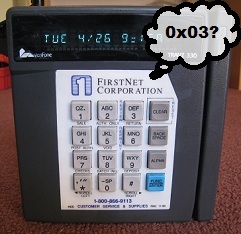
 I’ve finally made some visible progress in turning this Tranz 330 point-of-sale terminal into a general purpose Z-80 computer. It prints my name on the display! I may faint from the excitement.
OK, it’s not much to look at yet, but getting this far took a substantial amount of work in reverse-engineering the Tranz 330 hardware. Through tracing the circuit paths on the logic board, and examining the point-of-sale program in the terminal’s ROM, I slowly pieced together a map of where the peripheral devices are in I/O space, and how to communicate with them. Then after digging through the datasheets for the Z80 CPU, PIO, CTC, and the VFD display controller chip (all well-documented fortunately), I was ready to write a new program. I whipped up a tiny “hello world” program using a Z-80 assembler, burned it to my EEPROM, swapped out the original terminal ROM, and voila! There’s my name, in beautiful aqua-colored vacuum fluorescent glory.
I’ll provide more technical details in a bigger “how to” post once I have a more full-featured example. Until then, here are some of the minor problems I ran into, in addition to the job of reversing the hardware design:
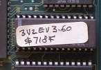
The original terminal ROM is a 32K UV-erasable 27C256. I’m sure not going to wait around to UV-erase my ROM each time I want to try a program modification, so I got a more modern 28C256 EEPROM as a replacement. The trouble is (and I didn’t notice this at first) the 28C256 is not exactly pin-compatible to the 27C256. Two pins are swapped. Where the Tranz logic board supplies +5 and A14, the 28C256 expects A14 and /WE. What the heck? It turns out I probably should have gotten a 27SF512 instead, which is a 64K part, but is drop-in compatible as long as you put the 32K image in the upper half.
I could almost fix my pin mismatch by bending some pins and adding some jumper wires, but modifying the 28C256 would prevent me from reprogramming it later. In the final result, I sacrificed a nice ZIF socket, cut off the /WE pin, jumpered /WE to VCC, and moved my program data to the upper half of the ROM where A14 = 1.
The original purpose of the ZIF was to avoid needing to socket and re-pull the ROM every time I wanted to test a change to my program. I put the ZIF in the motherboard’s socket, and the ROM in the ZIF. Unfortunately the ZIF fit the socket pretty loosely, and even more loosely after I cut it up, so it doesn’t work unless I press down on it with my thumb while it’s running. Ah, quality. I’m not sure what a better long-term solution is.
One last headache: my EasyPro 90B EPROM programmer apparently doesn’t work under Windows 7 64-bit. After searching for a while, I concluded there’s no appropriate driver, and I have to boot into XP whenever I want to program a ROM, which is a pain in the butt. I know nobody cares, but I can’t resist a chance to complain! If you’ve got a recommendation for a decent and not too expensive EPROM programmer that works under Win 7, please let me know.
Next step: some demos involving the keypad and speaker. Maybe a game of battleship?
Read 10 comments and join the conversationZ-80 Based Credit Card Terminal
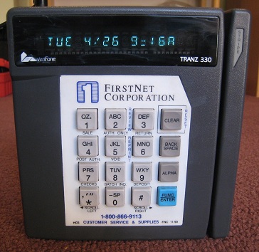 I found an old credit card terminal at an electronics surplus store recently, and bought it to tinker with. $5 at Weird Stuff in Sunnyvale! This Verifone Tranz 330 was used to process credit card transactions in the 80’s and 90’s, and is probably still used today some places. I wasn’t really interested in the credit card aspect though, but hoped to take it apart, learn how it works, and see if I could do anything interesting with it. Inside is a simple, self-contained 8-bit computer with a lot of hacking potential.
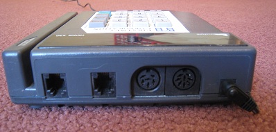
The Tranz 330 has a 16 key keypad, 16 character vacuum flourescent display (each charachter with 16 alpha-numeric segments), and a serial port with an 8 pin DIN connector. It also has an internal modem, a pair of telephone jacks, and a specialized 6 pin DIN serial port intended for use with peripherals. Lots of interesting interfaces to experiment with here.
Inside are two stacked circuit boards. The logic board contains a Z-80 CPU running at 4MHz, with a 32K socketed ROM, and 32K SRAM. The display board contains the VFD controller and keypad interface, as well as a piezo speaker.
So what do I do with this thing? It’s a full-on Z-80 based computer capable of lots of mischief, cramped only by the limited keypad and display. In theory, I could play Zork on this box. The socketed ROM would make it easy to replace the credit card terminal program with something of my own.
The challenge lies in determining the memory and I/O mapping used. How do you read the keypad? How do you write a character to the display? How do you work with the serial port or drive the speaker? I could dump the contents of the ROM and reverse-engineer the credit card program to find the answers. That’s probably the best way to go, but it sounds like a pain in the butt. I could also attach probes and examine the busses with my logic analyzer while the terminal is running. The logic and display boards are joined by a single 20 pin connector, so there’s not that much to analyze.
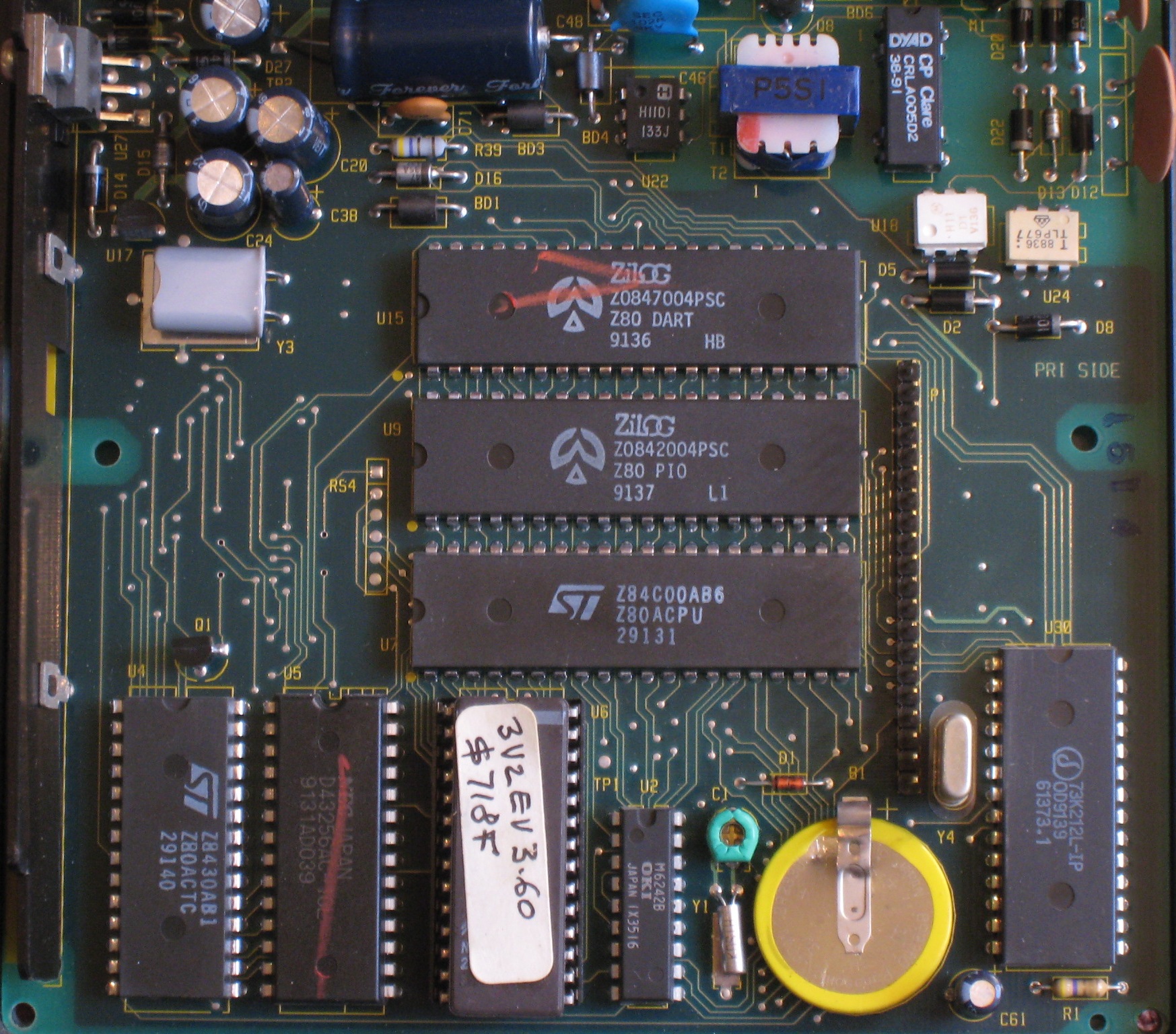
Meanwhile, let’s take a closer look at the components on the circuit boards, and see what’s there. Examining the CPU board first, in the center there’s the Z-80 CPU, PIO (parallel ports, probably used for the keypad and display), and dual UART (presumably used for the serial ports). Across the bottom row from left to right, there’s the Z-80 counter/timer, 32K SRAM, 32K EPROM, real-time clock chip, battery, and the single-chip modem. There are a few smaller chips at the top– I couldn’t learn anything about them, but by their placement I’m guessing they’re related to the phone interface.
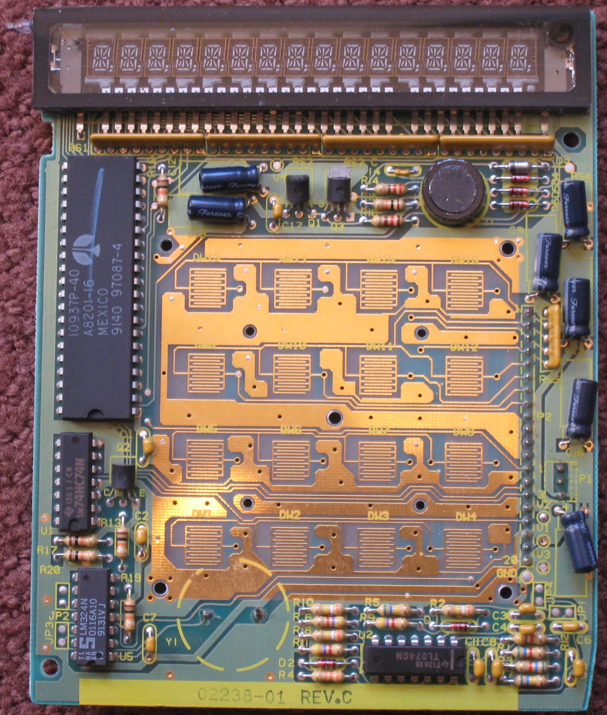
On the display board, examine the chips going counter-clockwise beginning with the largest chip. The large chip is the VFD display controller, a Micrel MIC10937. Following that is a dual-D flip-flop chip, a quad op-amp chip, and a second quad op-amp chip of a different type. I’m not sure what the eight op-amps are needed for– powering the VFD perhaps? Driving the speaker? Decoding the keypad key presses?
Post your best ideas for interesting hacks using this little box!
Read 33 comments and join the conversation