

Mapping the Tranz 330
 The VeriFone Tranz 330 point of sale terminal and its cousins are great platforms for electronics tinkerers. Commonly available from surplus stores or eBay for around $10, these little boxes contain a complete 8-bit computer, with lots of intersting I/O interfaces and a retro-styled vacuum-fluorescent display. The Tranz uses the Z-80 microprocessor, same as the venerable TRS-80 and ZX Spectrum, so software routines from those classic computers can often be reused.
The default program in the terminal’s ROM is a rather dull credit card processing application, but a new program can be substituted by replacing the original ROM chip. With knowledge of the hardware and a Z-80 assembler, you can write a new program to make the Tranz do any crazy thing you can imagine, like Mozart’s Credit Card: turning credit card magnetric stripe data into music. This guide will show you how.
Systems Specs
- Z-80 CPU at 4 MHz
- 32K ROM, in a socket for easy replacement
- 32K RAM
- 16 character, 16 segment vacuum fluorescent alphanumeric display
- 16 key 4×4 keypad
- Piezo speaker
- Magnetic stripe card reader, ISO 7813 Track 2 format
- Z-80 PIO, parallel port interface
- Z-80 DART, serial port interface
- Z-80 CTC, counter/timer
- OKI M6242B Real-time calendar/clock chip
- Micrel MIC10937 display controller
- RS-232 serial port, 8-pin DIN connector
- Accessory serial port, 6-pin DIN connector
- 73K212L-IP single chip 1200 bps modem
- Internal lithium battery backup for RAM
Related Tranz Terminals
VeriFone also produced several similar Tranz terminal models. I haven’t used these, but most of what’s written here about the Tranz 330 should also apply to them. Software written for the Tranz 330 may need small modifications to account for hardware differences on these other terminals, however.
- Tranz 380 – Z180 CPU at 6 MHz, 64K ROM, 64K or 128K RAM, track 1/2/3 card reader
- Tranz 460 – Z80A at 3.579 MHz, track 1/2 card reader, integrated receipt printer
Power Requirements
Used Tranz 330 terminals are often sold cheaply without the AC adapter, but fortunately replacements are inexpensive. The important thing to be aware of is that it requires an AC-to-AC adapter, not AC-to-DC. The stock VeriFone adapter outputs 8.5VAC at 1 amp. I have also successfully used Jameco part number 1586154, which is a 9VAC 1 amp adapter for $7.95. Any other similar adapter with a 2.5mm inner diameter should also work.
Why does the Tranz 330 use an AC-to-AC adapter instead of AC-to-DC? I don’t know, and I didn’t investigate. On-board power regulation is provided by an L387A low dropout 5V DC regulator, and all of the digital electronics use a 5V DC supply. Maybe this was a cost-saving measure of some kind?
I/O Board Interface
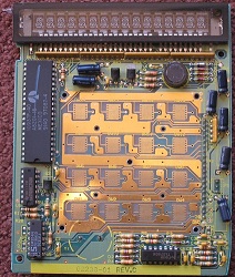 Inside the Tranz 330 case, the components are split between two circuit boards, stacked on top of each other and joined only by a single 20-pin 0.1 inch connector. The logic board is on the bottom, and contains the CPU, support chips, power supply, serial ports, and modem. The I/O board is on the top, and contains the keypad, display, MIC10937 display controller, and speaker.
For people using a microcontroller instead of the Z-80, the logic board can be discarded, and the I/O board and case used alone. The connection between the boards is not soldered, so they can be easily separated. This makes a nice self-contained I/O solution for a microcontroller project, with all the necessarily signals available at the 20-pin header.
I/O Board Connector Pinout
- keypad top row
- keypad second row from top
- keypad third row from top
- keypad bottom row
- keypad right-most column
- keypad second column from right
- keypad third column from right
- keypad left-most column
- NC
- NC
- NC
- card reader output
- display reset
- display data input
- display clock
- +5V DC
- speaker driver input
- -5V DC
- speaker mute?
- GND
Note pin 17 is actually connected to the clock input of a flip-flop in the speaker driver, and not directly to the speaker itself, and so the I/O board is only capable of playing square waves of various frequencies. Pin 19 is connected to the FF’s asynchronous set input. Pin 12 is the signal from the card magnetic read head, and must be decoded as described below in the section about the card reader.
Making a Replacement ROM
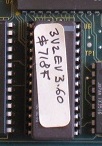 If you keep the logic board, you’ll need to replace the original ROM with one containing your new program. The original ROM is a 28-pin, 32K (256 kbit) 27C256 UV-erasable EPROM. Assuming you don’t already own a UV eraser and enjoy spending 15 minutes erasing your EPROM each time you change your program, you’ll want to replace this with a more modern 32K EEPROM or Flash ROM.
You’ll need an EPROM/EEPROM/Flash universal programmer to make your new ROM. If you don’t already have one, MCUmall has a good selection of inexpensive programmers. I use the EasyPro 90B.
Unfortunately no currently-manufactured EEPROM or Flash exactly matches the capacity, physical size, and pinout of the 27C256. The best solution is to use a 27SF512 Flash ROM. This is a 64K ROM, but if you place your program in the upper half (configure your programmer’s software to place the data at $8000), it is pin-for-pin compatible without any further work needed. Sadly, the 27SF512 is no longer manufactured, but is still commonly available from secondary sources and auto parts suppliers, since it’s a favorite of people who re-chip their car’s electronic fuel injection controller.
An alternative solution using all-new parts is to use a 28C256 EEPROM. This is a 32K ROM, but the pinout is slightly different than the 27C256. To make it work, after burning the ROM, pin 27 should be bent up and soldered to pin 28. Make sure that pin 27 does not contact the socket. Of course, this makes it impossible to reprogram the ROM later, so you may want to do this modification to a low-profile ZIF socket instead of the 28C256 itself. As before, you also must place your program in the upper half of the ROM (configure your programmer’s software to place the data at $4000). Since the 28C256 is a 32K device, this limits you to a total ROM image size of 16K. I used this method successfully until I found a supply of 27SF512 chips, but it can be difficult to get a reliable electrical contact between the ZIF and the underlying ROM socket.
Software Tools
Your program will be written in Z-80 assembly language, so you’ll need an assembler. I used sjasm, but any Z-80 assembler will work. You may also want a Z-80 simulator to help test your code before burning it to ROM. I used an evaluation version of Z80 Simulator IDE.
You may find some online references to “programming” the Tranz 330 in a propriety language called TCL. Ignore these. TCL is an ugly run-time interpreted language for making custom point of sale applications, and the interpreter is part of the original ROM. TCL programs run inside the sandbox provided by the interpreter. You’ll be making a native Z-80 program that has direct access to all the hardware.
Tranz 330 Library Routines
 While creating the Mozart’s Credit Card demo, I developed a set of reusable library routines for working with the Tranz 330 hardware. These routines simplify common tasks like printing a string to the display, reading the keypad, and playing a tone on the speaker. The file tranz330.asm contains all these library routines, as well as the Mozart demo program to serve as a working example. Use this as a starting point for making your own Tranz 330 programs. Portions of the library routines also appear below in the hardware-specific sections.
You can also download an archive containing the original Tranz 330 program file dump, my commented disassembly of the original program, and two versions of the Mozart demo in source and binary form.
Tranz 330 library routines Tranz 330 + Mozart archive
Memory Map
The Z-80 has a 64K memory address space. ROM is mapped to addresses 0 – $7FFF. At startup, program execution begins at address 0. RAM is mapped to addresses $8000 – $FFFF. Typically the stack will begin at $FFFF, growing downward.
I/O Ports
The Z-80 also has a separate 256 port I/O space. For the Tranz 330, these ports are mapped as follows (all port numbers in hex):
- Port $00 – PIO parallel port A.
- Bits 3-0: output, keypad columns. Bit 3 is right-most column.
- Bit 4: output, display controller reset
- Bit 5: output, display controller data
- Bit 6: output, display controller clock
- Bit 7: input, card reader data
- Port $01 – PIO control register for port A.
- Port $02 – PIO parallel port B.
- Bits 3-0: input, keypad rows. Bit 3 is bottom row.
- Bits 7-4: not connected
- Port $03 – PIO control register for port B.
- Port $10 – CTC channel 0
- Port $11 – CTC channel 1
- Port $12 – CTC channel 2. Chan 2 output is connected to speaker driver.
- Port $13 – CTC channel 3. Chan 3 input trigger is connected to chan 2 output.
- Port $20 – DART serial port A. 8-pin DIN RS-232 port.
- Port $21 – DART control register for port A.
- Port $22 – DART serial port B. 6-pin DIN accessory port.
- Port $23 – DART control register for port B.
- Ports $30 – $3F – Real-time clock registers $0-$F
- Ports $40,$50,$60,$70 – Modem?
Most applications will use the PIO parallel ports. Complete details on using the PIO can be found in the Z-80 PIO user’s manual. For the Tranz 330, this library routine will initialize the ports with the necessary settings:
system_init:

LD A,0xCF           ; control each port bit individually

OUT (0x01),A

LD A,0x80           ; bit 7 is input, others are outputs

OUT (0x01),A

LD A,0x18           ; use interrupt vector 18

OUT (0x01),A

LD A,0x97           ; generate interrupt if any masked bit is low

OUT (0x01),A

LD A,0x7F           ; interrupt mask = bit 7

OUT (0x01),A

LD A,0x3F           ; set the initial output values for port 0

OUT (0x00),A

RET
Display
![]() The 16-character, 16-segment VFD is powered by a Micrel 10937 display controller. It supports upper-case letters, digits 0-9, and a small selection of symbols.
The 16-character, 16-segment VFD is powered by a Micrel 10937 display controller. It supports upper-case letters, digits 0-9, and a small selection of symbols.
The controller is connected to the CPU through a serial interface, using port $0 bits 6-4. Data bytes must be shifted in to the controller one bit at a time. The serial clock must also be toggled via software for each bit. Data bytes are 8 bits, and are transmitted MSB first. An MSB of 1 indicates a control byte, and an MSB of 0 indicates a data byte to be displayed.
After a reset, the display is turned off by default. Before printing anything, it must first be turned on by setting the display duty cycle to something higher than zero.
display_init:

IN A,(0x00)         ; get current port state

AND 0xEF            ; clear bit 4 (display reset)

OUT (0x00),A

LD B,0x1C           ; wait 0x1C cycles

.L1 DJNZ .L1

OR 0x10             ; set bit 4 (display reset)

OUT (0x00),A

LD C,0xFF           ; set the display duty cycle to 31 (maximum brightness)

CALL display_send_byte

RET
Sending a control or data byte to the display requires shifting it out one bit at a time on port $0 bit 5, while toggling the serial clock on port $0 bit 6:
display_send_byte:

; byte to be sent is in C

; note the display controller does not support lower-case letters!

LD B,0x08           ; 8 bits to send

.L1 IN A,(0x00)         ; get current port state

RLA                 ; rotate the port word until the data bit is in the carry flag

RLA

RLA

RL C                ; shift the next output data bit into the carry flag

RRA                 ; rotate the port word until the data bit is in bit 5

RRA

RRA

OUT (0x00),A        ; setup the data output (bit 5)

OR 0x40             ; set clock high (bit 6)

OUT (0x00),A

AND 0xBF            ; set clock low (bit 6)

OUT (0x00),A

DJNZ .L1            ; continue with the next bit

RET
Keypad
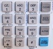 The 16-key keypad is arranged in a 4×4 layout. It contains a 12-key telephone-style section with the digits 0-9, *, and #, as well as the four special function keys CLEAR, BACKSPACE, ALPHA, and ENTER. The keypad is a passive device, requiring work from the CPU to test the keypad state. The keypad has four column lines and four row lines, and the row lines have pull-up resistors. When a key is pressed, an electrical connection is made between the row and column lines that overlap beneath that key.
By driving a 0 to a single column line while driving a 1 to the others, the CPU can activate that column. The current state of the four keys in that column can then be tested by reading the row lines. If a key in an active column is pressed, the corresponding row line value will be 0. If no key is pressed, the pull-up resistor will supply a value of 1 for that row. To detect key presses, the CPU must activate each of the four column lines in turn, and check the row lines for 0’s.
The column lines are connected to the CPU on port $0 bits 3-0, and the row lines on port $2 bits 3-0.
The library function keypad_read returns a key code in the range 1-16 in A, or 0 if no key is pressed.
To enter a multi-character string involving letters, numbers, and symbols, a higher-level input routine is needed. The library function keypad_get_string reads a complete string from the user, and provides some basic line editing capabilities. Key presses are echoed to the display. BACKSPACE can be used to correct mistakes. Letters and special characters can be entered by first pressing a number key, and then repeatedly pressing ALPHA to cycle through the alternate characters for that key. String entry concludes when ENTER is pressed.
CTC and Speaker
The Z-80 CTC has four independent counter/timer channels, addressable by the CPU on ports $10 – $13. Complete details on using the CTC can be found in the Z-80 CTC User’s Manual. The channels can be configured to trigger an interrupt when timeout occurs. Each channel also has a timeout pin and a trigger pin for direct hardware interfaces. On the Tranz 330, the channel 2 timeout pin is connected to the clock input of a flip-flop in the speaker driver, and also to the channel 3 trigger.
A square wave tone of any desired frequency can be played through the speaker by setting an appropriate time constant on channel 2. Unfortunately, there’s no way to control the volume or create other audio waveforms.
To configure channel 2 for speaker usage, it must be set to timer mode with auto-triggering. The desired frequency can then be played by loading an appropriate time constant into channel 2:
speaker_beep_period:

; beep tone period time constant should be passed in C

LD A,0x07           ; disable interrupts, timer mode, prescale=16, auto-trigger, time constant follows

OUT (0x12),A

LD A,C              ; time const

OUT (0x12),A        ; speaker on

LD BC,0x0096       ; wait 150 ms

CALL wait_ms

LD A,0x03

OUT (0x12),A        ; speaker off

RET
Card Reader
The card reader supports ISO 7813 Track 2 format, which is up to 40 characters, where each character is 4 data bits and one odd parity bit. It will read virtually any credit card, driver’s license, shopping card, ID card, or other card with a magnetic stripe. Typically the data on the magnetic stripe is the same as what’s printed on the card: account number and expiration date. In many cases, depending on the type of card, some additional data may be stored as well. The magnetic stripe does not contain PINs or other private data.
The card reader is connected to the CPU on port $0 bit 7. The port is configured to trigger an interrupt whenever the card reader signal is active. At the CPU interface, the card reader signal is normally 1 when no card is present, and toggles rapidly between 1 and 0 when a card is swiped. If you’re using the I/O board with a microcontroller and directly sensing pin 12 from the 20-pin header, then the polarity is reversed: the signal is normally 0, and toggles rapidly between 1 and 0 when a card is swiped.
Interpreting the card reader signal is complex, because there is no clock signal, the speed at which the data signal changes depends on the speed the card is swiped, and because the signal doesn’t even directly provide the logical binary data from the card.
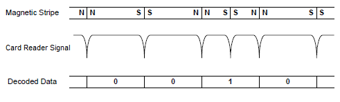 A track on the magnetic stripe consists a long series of magnetic domains. Each domain is polarized magnetic North or South. When the read head is over a domain of either polarity, the card reader signal is 1. When the read had passes over the boundary between domains of opposing polarities, the card reader signal briefly pulses to 0. The duration of this pulse is approximately 40 microseconds.
Each logical data bit on a track has the same physical length on the magnetic stripe. There will always be a magnetic domain boundary at edge of a bit. A logical 1 bit will also have a magnetic domain boundary within the length of the bit, but a logical 0 will not. Extracting logical 0’s and 1’s is therefore a task of measuring the intervals between pulses of the card reader signal. Two successive pulses each time N since the last represent a logical 1, and a single pulse time 2N since the last represents a logical 0. This encoding format is called F2F or Aiken Biphase.
The data begins with a long string of logical 0’s, enabling the software to calibrate the value of N for that swipe of the card. For better reliability, the card reader library routine also adjusts the value of N during bit transcription, to compensate for an accelerating or decelerating motion during the card swipe.
Using the library routines for the card reader is a multi-step process:
- At startup, system_init sets the interrupt handler to be called when the card reader signal pulses low.
- The interrupt handler uses a busy loop to measure the duration of each 0 to 1 cycle of the card reader signal, storing the duration data in a buffer. When the handler terminates, control is returned to the routine got_card.
- card_parse_bits is called to perform the F2F decoding of the duration measurements, filling the buffer with logical 0’s and 1’s.
- card_parse_characters is called to convert the logical bits into ASCII characters, filling the buffer with a null-terminated ASCII string. The ASCII conversion adds $30 (ASCII ‘0’) to each 4-bit datum. If a parity error is detected, the empty string is returned.
The final string returned will begin with a start sentinel (ASCII ‘;’), contain up to 40 characters of content, and end with an end sentinel (ASCII ‘?’). The data content typically begins with the account number (up to 16 characters), followed by a ‘=’ field separator, expiration date in YYMM format, and finally other data specific to the card provider.
Serial Ports
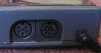 The Tranz 330 has two serial ports: an RS-232 port with 8-pin DIN connector, and an accessory serial port with 6-pin DIN connector. The serial ports are controlled by the Z-80 DART, which is basically a Z-80 SIO/0 without the synchronous clocking capability. Complete details on using the DART can be found in the Z-80 SIO User’s Manual.
The serial ports are connected to the CPU via the DART on ports $20 and $22. Port $21 is the control register for port $20, and port $23 is the control register for port $22.
I didn’t experiment with the serial ports or write any library routines for them, so people wishing to use the serial ports will need to consult the SIO User’s Manual and write the code themselves. Usage is fairly straightforward: write to port $21 to set the serial port direction and speed, then read/write data from/to port $20.
Real-Time Clock/Calendar
The OKI M6242B real-time clock provides a mechanism to query and update the second, minute, hour, day, month, and year. Because the Tranz 330 has an internal backup battery, the date and time is retained even when external power is lost. The M6242B has 16 control registers, which are mapped to CPU I/O ports $30 – $3F. Complete details on using the RTC can be found in the M6242B datasheet.
Internal Modem
The 73K212L-IP single-chip modem provides a 1200 bps interface for communication over dial-up phone lines.
I didn’t experiment with the modem or write any library routines for it. From examination of the original Tranz 330 ROM program, I believe the modem is connected to the CPU on one or more of I/O ports $40, $50, $60, and $70. Complete details on using the modem can be found in the 73K212L datasheet.
Feedback
If you find this technical information useful, and make a cool project based on the Tranz 330, please leave a note in the comments!
Errata
The following information was contributed by John Barthol.
The port addresses are correct in your documentation but the SIOA port is mapped to some pins on the modem chip (not the 8 pin DIN). I found that the 8 pin DIN was mapped to SIOB. The pin pad (6 pin DIN) port is mapped to SYNCB on the SIO and one of the pins on the PIO. The system clock speed is 7159090 so the CTC trigger clock is 1/4 of that or 1789772.5. Baud rate can be calculated by BAUD = 1789772.5 / (CTC_TIME_CONSTANT * DART_SCALE_FACTOR). I ended up using a time constant of 186 and scale factor of 1 to get me to 9600 baud. Actual baud is 9622 but it seems close enough.
Read 16 comments and join the conversation16 Comments so far
Leave a reply. For customer support issues, please use the Customer Support link instead of writing comments.
Steve,
I read about your Mozart project on hackaday and immediately went to ebay looking for one of these. Thank you for taking the time to map everything out so that those of us less experienced with such devices can still have some fun with them. I’m wondering if it would be possible to interface some form of non-volatile storage to the device for storing card numbers? Better yet, when I replace the rom with an eeprom, could I edit non firmware addresses of the eeprom to store data in real time? I may be better off to just interface a microcontroller with built in eeprom, but, on the other hand, this would be a good chance to familiarize myself with assembly.
Thank you for the work you have put into this project!
I think it would be a challenge to add non-volatile storage. What kind of data do you want to retain? No, unfortunately the hardware can’t write to it’s own EEPROM/Flash. The RAM is battery-backed, so you can use that for storage as long as you’ve got a good battery.
Couldn’t you use the spare pins (bits 7-4) on PIO port B for bitbanging SPI to connect a serial EEPROM such as an AT25040B ?
I’m not sure how you could physically connect something new to PIO port B. You’d probably have to solder wires directly to the PIO pins, with the PIO itself still soldered into the logic board.
Thanks for the replies Steve and Jonno. I actually have neat little idea for a keycard entry system. I can use my university id to open my door in the dorm I live in now, but the dorm I will be staying in next year has traditional locks. A bit low-tech for my taste. The idea is to mount one of these outside my door and use it to operate a remote door opener on the inside. Of course, the remote opener will have to have some “smart” circuitry as well so that someone can’t just open the panel and hotwire this thing. That, or I relocate the mainboard to the other side of the door. I guess the ram might be sufficient for what I need if the battery life is good. Theoretically, our school should never loose power anyway. I would store an administrative password as well as authorized keycards and maybe some short messages that the unit would display when its just sitting there. I could hardcode all this, but non volatile storage seems more professional.
Got my Tranz 330 in the mail last night and wasted no time firing it up. Will be a while before I can start my project, but I wanted to make sure it was in working order. For the record, I was able to power it using 8.5V DC. Polarity made no difference. Anyone know if it could possibly damage the Tranz 330 to use DC long term? I can’t think of any reason why DC might damage the device. It would seem the supply is immediately converted to DC anyway.
I agree, it looks like the supply goes immediately through a rectifier to a DC regulator, so DC should work as well as AC. I really can’t explain why the original power supply is AC. Maybe some of the peripherals required AC power?
The built in modem opens up all sorts of possibilities! Could several of these be neworked together to create some sort of distributed computing cluster?
It perplexes me how the mainboard generates the -5v which feeds the IO board (probably for the vfd). I only see one regulator on the whole board, the L387A. I did notice that there were two bridge rectifiers. Perhaps the -5v is unregulated? Using two separate rectifiers to generate two dc polarities would explain the use of an AC supply, but how is it that I was able to power this thing using DC above? Any thoughts? This thing has me stumped 🙁
Do you know if the DUART’s Port A is initialized to work like a regular RS232 port when the device is initialized, or is there a requirement for me to set registers? I’ve been looking at the DUART data sheet and the different options that one can set are just discombobulating. The worst part about is is the fact that I have no idea where the DUART frequency is derived from – the 4 MHz main oscillator?
As for cool uses for this thing – I’m screwing it to my door in my new house and using it to lock/unlock my door by communicating all card data and friends to another micro controller that logs this and then does the actual unlocking. Plus this is a fun little project for me to learn Z80 ASM =P
I have tried many times to setup the Tranz 330’s Zilog Z80 SIO dart. Just so confusing on the Zilog’s users guide on how to setup the SIO. Like the baud rate generated from the CTC looks to be around 38KHz on channel 0 on the original software no matter what baud rate you are running. So looks like there is A devisor to input in who knows what register on the SIO. Just confused on where to setup the devisor on the SIO. The data in the Zilog document again is so mind discombobulating on this setup. As there is no mention of any type of devisor like other SIO devices.
Do you have any example code on this SIO. Or if not where might I get A clue on this. As I have tried to reverse some of the original code. But some decompilers get kinda hard to decipher code from data and one can get lost quickly in all that code. Help
Thanks Richard
John Barthol sent me some corrections and additions to the Tranz 330 I/O mappings, which I’ve added above in the Errata section. Thanks John!
Initially I thought the AC adapter was used to provide the AC voltage to the VFD filament, on the cheap. BOSE is especially bad for that.
I got my trans330 in. I know why it has an AC adapter. there are dual rectifiers. a positive one for the 5V, and the negative rectifier for the 79L05 which is used to create the -5V required for the op-amps and the modem/serial.
I am not quite sure why but when I modified my ROM image recently (containing a custom monitor with Intel hex loader, Micro-soft 8K basic and Steve’s Mozart program), my ROM image would just hang and I never got my main menu on the Tranz after powering up, just a blank display and no serial communication. I noticed in Steve’s disassembly that there is an init_delay loop just before the stack pointer is loaded in the original ROM disassembly. Once I added that code to the ROM everything started working again.
This makes a great little z80 development system. My latest project was recreating Steve Dompier’s Fool on the Hill for the Altair. For some reason I cannot pick it up on AM but I can tune it in on FM.
My next project is going to be either making a calculator or alarm clock out of this thing. I’ll probably do both. Does anyone have any pointers to some good math libraries for the Z80?
Thanks!
JB
Is the mag stripe head capable of writing magnetic data to cards?