

Archive for the 'Dev Tools' Category
Atmel-ICE + Floppy Emu. The Taste of Sadness
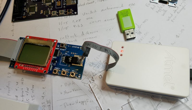
In all the time I’ve been developing Floppy Emu, can you believe I’ve never had a debugger? I use the Atmel AVRISP mkII to program the Emu’s ATMEGA1284 microcontroller, but the mkII only supports programming and not debugging. I don’t have a serial port or other logging mechanism either, so when I encounter mystery problems, I need to debuga them by displaying one-time error codes or blinking an LED. Not very convenient.
Last week I finally purchased a proper debugger – the Atmel-ICE. It supports both JTAG and debugWIRE debugging, which are the two interfaces used in the ATMEGA family of microcontrollers. The Atmel-ICE also supports Atmel’s SAM family of 32-bit ARM microcontrollers, which will be handy if/when I start working with those.
With excitement, I connected the Atmel-ICE to Floppy Emu’s 6-pin ISP port. I was able to communicate with the ATMEGA1284 chip, view its fuses, and reprogram it. Visions of breakpoints and memory dumps danced in my head – this was going to be awesome. Then I started a debug session, only to encounter this error:
Use Start Without Debugging to avoid this message.
Wha-wha-what? Does not support debugging??
I searched in vain for a debugWIRE option, but the only interface choices displayed by the software were ISP and JTAG. After a frantic documentation search I discovered the sad truth. I’d thought the ATMEGA1284 had both debugWIRE and JTAG debugging interfaces, but the presence of JTAG actually means the chip doesn’t support debugWIRE. Even though the necessary debugWIRE pins are right there, and debugWIRE is mentioned in the chip’s datasheet, and there’s a debugWIRE enable fuse on the chip. Ugh.
I confirmed that a test project configured for the ATMEGA328P causes the debugWIRE option to appear in the Atmel Studio software. But Floppy Emu doesn’t have a ATMEGA328P. As soon as I change the project’s device type to ATMEGA1284, the debugWIRE option disappears.
Unfortunately I can’t use the JTAG interface, because I didn’t plan for it, and there’s no JTAG connector on the Floppy Emu board. I can’t do micro-soldering surgery to create a JTAG port either, because the ATMEGA1284 JTAG pins are connected to the board’s Xilinx CPLD chip, to support runtime reprogramming of the CPLD.
I’ll continue debugging with a blinking LED. Debuggers are for wimps. 🙂
Read 2 comments and join the conversationQuest For a Simple JTAG SVF Player

Where are all the cheap and simple third-party JTAG programmers? My work on the Yellowstone disk controller was sidetracked by issues with the Lattice-clone JTAG programmer, and discussion about ways that future Yellowstone customers might do JTAG programming. Eventually I realized that any generic JTAG hardware can program Yellowstone’s Lattice FPGA using a standard SVF file generated by the Lattice software. But what JTAG programming hardware to use, and what software to control it?
The device I’m imagining needs to play SVF files on a JTAG interface and verify the result. That’s all. It doesn’t need to handle JTAG debugging, ISP programming, SPI, or anything else. It should have easy cross-platform software to control the device: a basic GUI where the user can select an SVF file and click a button, then see progress info and a final good/bad result. Since JTAG is a fairly simple serial interface, this shouldn’t be much more difficult than building something like a USB-to-serial adapter, along with software to control it, which could leverage something like lib(X)SVF for SVF parsing. I confidently assumed there would be many such devices available for sale.
I was wrong. My search found nothing that really fit the requirement of cheap and easy, though a few options came close. Here’s a summary of what I found. If I’ve overlooked something obvious, please leave me a note in the comments.
Bus Blaster – A $35 open source JTAG tool based on the FT2232H. The hardware fits the bill, but the software does not. The Bus Blaster seems mainly intended to be used with UrJTAG or OpenOCD software, which are both unfortunately the opposite of user-friendly. From what I can tell, neither one has an official binary distribution and must be compiled from source code. From there it’s a somewhat daunting sequence of command line work to get things done. Surely there’s a simpler option if all that’s needed is an SVF player?
Flash Cat – A $30 commercial JTAG device that also does SPI, I2C, and serial. It’s not clear what IC it uses. This might almost work, and the software looks promising, but it’s Windows-only.
TinyFPGA Programmer – A $9 open source programmer for the TinyFPGA product line, and based on a PIC microcontroller. This is the best solution I’ve found so far, and the software is simple and cross-platform. But the hardware is specifically designed for the TinyFPGA boards, and so it makes assumptions about voltage levels and JTAG pinouts, and may have other limitations that prevent it from being a general-purpose programmer. The software is a python module and the GUI is Tk. Beggars can’t be choosers, especially for only $9, but a native control program for Mac and Windows would be preferred.
Those were the only decent commercial options I could find. Everything else was either a platform-specific tool, or a more complex and expensive JTAG debugger like the Segger J-Link, or somebody’s one-off hobby project.
Am I blind, and overlooking an obvious solution? If not, why doesn’t something like this already exist? Is it more complicated than I imagine? Or is there simply no demand for it? It sure looks like you could build a device like this using any simple microcontroller or USB-to-serial converter. Then spend a little time creating native apps for Mac and Windows, and get everything lined up regarding necessary drivers and software signatures, and you’d have a very desirable product. I have half a mind to drop everything and go do this myself.
Read 9 comments and join the conversationZeroplus LAP-C 322000 Logic Analyzer Review
Who needs a logic analyzer? You do! If you enjoy working with electronics, a good logic analyzer is an indispensable tool. It lets you examine exactly what’s happening with your data signals, so you can troubleshoot problems quickly or reverse-engineer unknown protocols. Developing digital electronics without a logic analyzer is like navigating without a map.
In decades past, logic analyzers were bulky and expensive purpose-built machines from companies like Hewlett Packard. There’s still a place for such high-end equipment, but today most engineers can get everything they need from a small USB device that costs just a few hundred dollars. Saleae is one of the better-known names here, but it’s a crowded market with many worthy competitors. Which one is right for you?
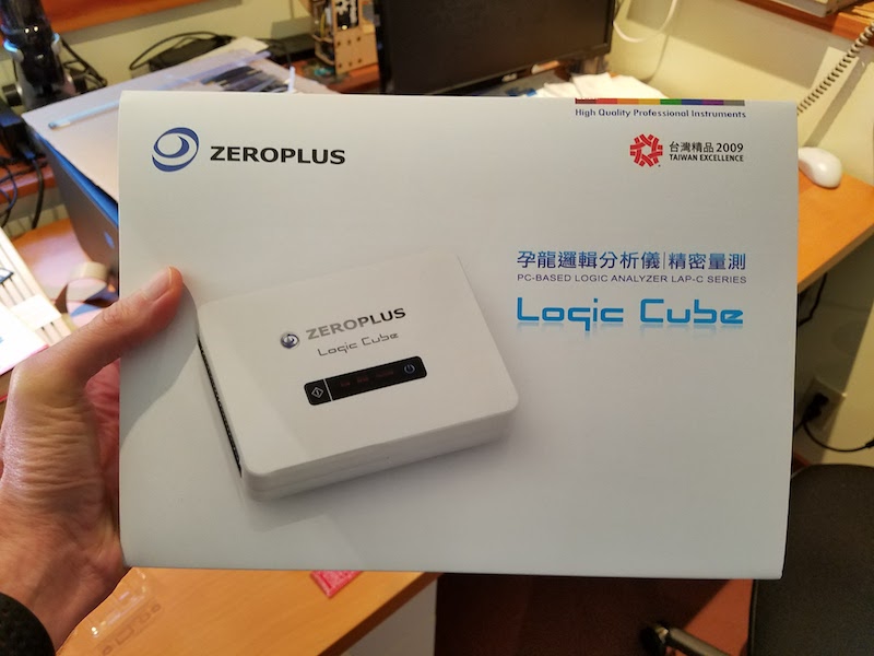
Hello Zeroplus
Today I’ll take a look at an example of the Zeroplus “Logic Cube” series. Zeroplus is based in Taiwan, and their logic analyzer products have a good reputation among Taiwanese IT companies, but are less well known in the West. Full disclosure: Zeroplus sent me a demo unit for the purpose of this review. What you’ll read below are my own unfiltered opinions of the hardware’s strengths and weaknesses.
The members of this product family are buffered logic analyzers, with a few megabits of high speed on-board memory for storing the captured sample data. This is the more traditional approach to designing a logic analyzer, and it provides some advantages versus the on-the-fly USB streaming approach used by Saleae and other similar low-cost logic analyzers. Buffered LAs aren’t reliant on the PC’s USB bandwidth, so they can capture many channels at high sample rates without fear of saturating the USB link and losing data. The tradeoff is that buffered LAs have finite storage space, so the maximum amount of data that can be captured is limited. Data compression helps, but once the on-board memory is full, signal acquisition stops. In contrast, streaming LAs support “infinite” capture sizes limited only by the PC’s available RAM and disk space, but have limited bandwidth.
The Zeroplus logic analyzers in this Logic Cube series are commonly called “LAP-C” for the common prefix in all of their model numbers, and you’ll find the most pertinent resources on the web by searching for this term. LAP-C models are sold in seven different versions, differing mainly in the number of channels and amount of on-board memory. For this review, I tested the top of the line LAP-C 322000, with a retail price of $1699 in the United States. Here are the specs:
Logic Analyzer: Zeroplus LAP-C 322000
Number of Channels: 32
Sample Memory: 64 Mbits (2 Mbits per channel)
Max Sample Rate: 200 MHz
Vinput of Testing Channels: -30V to +30V DC
Retail Price: USD $1699
In comparison, the mid-range members of the LAP-C family pare back the number of channels and memory size in exchange for lower prices. For example, LAP-C 16064 is 16 channels / 1 Mbit / 100 MHz for $249, and LAP-C 16128 is 16 channels / 4 Mbits / 200 MHz for $399.
Unboxing and Hardware
While the front of the box has English text, the technical bullet points on the back are primarily in Chinese. This probably doesn’t matter much, since very few people will ever be browsing store shelves when shopping for a logic analyzer, but it shows that Zeroplus’ marketing team has additional translation work to do if they hope to attract more Western customers.
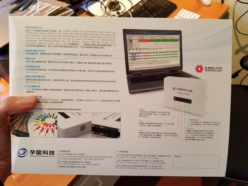
The 34-page instruction manual inside the box is also Chinese, but a well-written English-language manual can be downloaded here.
The logic analyzer unit and its accessories all fit inside a hardshell zippered case that’s included. While it’s a small thing, this is a very nice touch, and it makes it easy to pack up your project when you’re finished debugging hardware. The pulse width trigger module included with the LAP-C 322000 model is the only accessory that doesn’t go in the hardshell case.
The LAP-C 322000 package includes:
- logic analyzer main unit
- USB cable
- 32 flying lead wires
- 36 IC test hooks
- printed manual (Chinese)
- installation software CD
- hardshell case
- pulse width trigger module
- hookup wires for trigger module
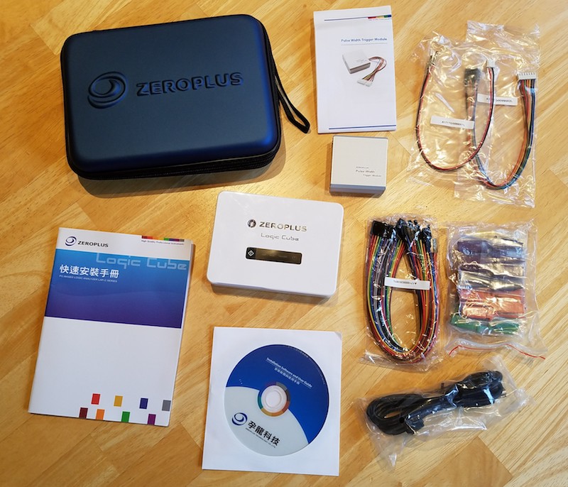
The pulse width trigger module is made from brushed aluminum. When connected to the main unit, this module upgrades the logic analyzer with a new feature: the ability to trigger on a high or low pulse whose duration is outside a user-selected range. This may be useful when working on PWM applications like dimmable lighting.
The main logic analyzer unit is made from an attractive gloss white plastic. The external interface is minimal: a button to start immediate captures, and status lights for Run, Read, and Trigger. The external connector is two rows of standard 0.1 inch male headers. In addition to the 32 data channel connections and ground pins, there’s also an external clock input, and a few special I/O pins for connecting the pulse width trigger module or a second LAP-C unit.
The LAP-C does not offer any analog measurement capability. While serious analog work demands an oscilloscope, some newer logic analyzers are starting to add low-bandwidth analog capability too. This can be useful for verifying that signal voltage levels are in a valid range, or that power supplies are behaving as expected. Analog measurement is a nice extra feature, but its absence here isn’t a deal-breaker.
Software
The LAP-C software is Windows-only. That’s not a big limitation, since any halfway-serious engineer will have access to a Windows machine even if it’s not their main system, but Macintosh and Linux software versions would have been nice. Windows 7, 8, and 10 compatibility is advertised. I used software V3.13.05 with Windows 7. You can download the software and try it out in demo mode, even if you don’t have the LAP-C hardware. The English-language software translations are generally well done and easy to understand.
The graphical interface appears geared towards advanced users, with a very large number of tools, measurements, and options visible directly on the main screen. This is great for power users, but may be overwhelming for newbies, or to anyone accustomed to the minimal interface of Saleae’s software. I found it a bit daunting at first, but after 30 minutes of experimenting and checking the manual, I had mastered the basics.
Some aspects of the UI would benefit from more polish. When viewing large data ranges, panning and zooming the waveform can be glitchy, with a laggy response to mouse input and different portions of the waveform scrolling a fraction of a second after others. Compared to the smooth pan and zoom of competing logic analyzer software, or to tools like Google Maps, that’s a little disappointing. Other minor graphical glitches and goofs sometimes appear, like waveforms that aren’t a uniform height or scale values that are the wrong units. The intervals of the ruler are also oddly chosen, with tickmarks at 0.409374912 seconds followed by 1.91042 seconds and then 3.411465 seconds, instead of divisions at even intervals using powers of 10. None of this prevents you from analyzing captured sample data, but it can be confusing and distracting.
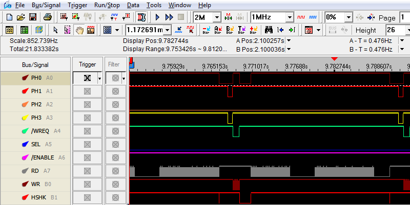
A data capture can be started immediately by pressing a button in the software, or by pressing the physical button on the logic analyzer unit. Captures can also be triggered by a level or edge condition on a single channel, or by more complex functions like a specific value on a parallel bus, or a protocol-level event like an I2C NACK.
There are an impressive number of powerful features embedded in the LAP-C software. Repetitive run triggers the logic analyzer over and over, so you can look for one instance that’s different from the others. Noise filter ignores pulses with a duration below the threshold you specify. Data can be captured with an asynchronous internal clock, or synchronously using an external clock connection. Captured data can be searched in several different ways to find a region of interest. Waveforms and data can be imported and exported for additional examination with other tools. There are many more advanced analysis features that I didn’t have time to explore deeply. Some of these may only be valuable in specific circumstances, like the memory analyzer for examining address/data information, but they’re great when they provide the special capabilities you need.
One small but curious shortcoming: in the software’s list of choices for the sampling rate, it skips directly from 1 MHz to 10 MHz with no intermediate options. Most of my electronics projects operate a speeds faster than 1 MHz but slower than 10 MHz, so the missing sample rate options are a bigger issue for me than they might be for others.
Capturing and viewing sets of raw waveforms is great, and is the core of logic analyzer usage. But to really get the most out of the tool, you’ll want to use the software’s protocol analyzers to provide a high-level representation of the data. A protocol analyzer is a software module that converts raw waveforms into decoded data packets. For example, if the software offers an I2C protocol analyzer, then you can view the captured sample data as a series of device addresses, data bytes, and ACKs, instead of counting raw transitions of the SCK and SCL signals while you thumb through an I2C reference guide. The LAP-C software offers over 100 protocol analyzers, including I2C, SPI, serial (RS-232C/422/485), JTAG, PS/2, USB, 1-WIRE, CAN, IRDA, 3-WIRE, and many more. Some of these used to be extra cost options, but since 2016 all the protocol analyzers are available free. Here’s a typical protocol analyzer example from Zeroplus:

How Much Sample Memory Do You Need?
When purchasing a buffered logic analyzer, you need to predict in advance how much sample memory you’re likely to need. Underestimating is bad: if there’s not enough sample memory, you won’t be able to capture as many channels for as long a duration as needed for your debugging work. But overestimating is bad too: it means you’ll pay hundreds of dollars extra for additional sample memory you don’t need. So how can you decide how much memory is enough?
This is a difficult question to answer, because it depends heavily on the type of electronics work that you do. You might work primarily with low speed serial signals, or you might need to analyze a wide parallel bus running at high speeds. Your data might be highly compressible with the LAP-C’s compression algorithm, or it might not. This leads to a frustrating “it depends” answer that satisfies no one.
For my own hobby electronics work over the past few years, I typically need to analyze systems with 5 to 10 signals running at speeds between 1 MHz and 10 MHz. My normal work pattern with a streaming logic analyzer is to manually start the capture, and record a few seconds of data, then examine it afterwards to zoom in on the interesting parts. Using a buffered logic analyzer, without the benefit of compression, this would require a worst case of 10 signals times 10 MHz times 10 seconds, or 1000 Mbits total. My simple experiments with LAP-C compression found that it provided about a 10x improvement for my data, so that reduces the memory requirement to 100 Mbits – close enough to the LAP-C 322000’s 64 Mbits. So with the top of the line LAP-C model, I could probably support my existing work pattern, but anything with less memory would be insufficient.
To really get the benefit of the LAP-C hardware, I would need to stop using 10 second long captures, and instead set up triggers to capture only the few hundred milliseconds or microseconds I’m really interested in. That would require some extra time for setup, but would greatly reduce the amount of memory needed.
Other Thoughts

Zeroplus’ web site lists two official US distributors, and one appears to only stock the entry level LAP-C 16032, leaving a single source for most LAP-C models in the US. With a bit of Google searching, you can also find third-party LAP-C sellers from Asia who will ship directly to the US. Direct sales from the Zeroplus web site would be a welcome addition, but are not currently an option.
Is the Zeroplus LAP-C series right for you? It depends on what you plan to do with it. For the casual electronics hobbyists who are typical readers of this blog, the $1699 price tag of the LAP-C 322000 may be more than they’re willing to spend, but they probably don’t need all the features of the LAP-C 322000 either. Zeroplus offers three LAP-C models with slightly lower specs all priced below $400, which are probably a better fit for part-time garage hackers. I expect that most hobbyists will be fine stepping down from 32 to 16 channels, although stepping down from 64 Mbits of memory to 4 Mbits or 1 Mbit may be a concern.
With 4 Mbits and 16 channels, at a 10 MHz sample rate and using compression, you’ll get a capture window of a couple hundred milliseconds. That’s small enough so that manual triggering is unrealistic. Instead, you’ll need to plan ahead of time to decide what your goal is with this capture, and how you can construct a trigger to capture exactly the region you need to examine. For power users working with high speed systems and large numbers of channels, this will already be familiar. They’re more likely to know specifically what they’re looking for, and to see complex trigger setup as a normal and expected part of debugging. They’re also more likely to benefit from some of the LAP-C’s advanced features and hardware options like external clock input, pulse width triggering, and detailed software analysis. The breadth and depth of the LAP-C software’s various tools and analyzers is impressive, and will surely be a boon for hardcore electronics engineers. Beginners and others with more basic needs may be better off with an 8-channel streaming logic analyzer with a simple and friendly software interface.
What about the general merits of buffered vs streaming logic analyzer designs? For situations where there’s enough USB bandwidth to stream the sample data on the fly, I believe that approach provides a better user experience. There’s no need to worry about trading off sample rate for sample depth, or worrying whether the capture window will be large enough to contain all the events of interest. But for more demanding situations with large numbers of channels and high sample rates, streaming just doesn’t work. 32 channels at 200 Mhz sampling rate is 6.4 Gbits/sec, which is more than USB 3.0’s total maximum theoretical bandwidth and far more than its real-world bandwidth. So depending on the application, both streaming and buffered designs have their place.
My ideal logic analyzer would be one that operates in streaming mode where sufficient USB bandwidth is available, and falls back to buffered operation when streaming won’t work. That would probably be needlessly complex and expensive, but I can dream!
Read 4 comments and join the conversationPIC32MX Mini-Review
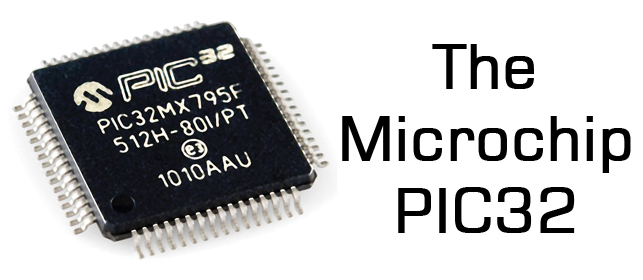
Now that I’ve been using a PIC32MX microcontroller for a while, and its associated software tools from Microchip, it’s time for a mini-review. My previous microcontroller experience was primarily with 8-bit Atmel AVRs, so my comments will reflect that. Many of the differences between a PIC32MX and AVR will also apply to any other modern 32-bit microcontroller, like the many ARM variants.
On the whole, I’ve been fairly pleased with the PIC32MX. Below you’ll see that I’ve written much more about dislikes than likes, but that’s because the likes are largely self-explanatory, while the dislikes deserve a more detailed explanation.
Note: Last year Microchip purchased Atmel, the makers of the AVR. So now both of the microcontrollers in my comparison are provided by the same company.
HARDWARE LIKES
Faster core speeds – Up to 50 MHz on my PIC32MX230F256, 80 MHz on other devices in this family.
Clock PLL – Synthesize core speeds anywhere from 1 MHz to 50 MHz from a fixed-speed external crystal or internal RC oscillator.
More flash memory – 256KB seems like a lot.
Configurable pin remapping – Relocate functions like the UART’s TXD and RXD to one of several different possible physical pin locations. Makes PCB routing much easier.
Set / clear / invert registers – Modify a single GPIO pin with a single instruction, without needing to do a read-modify-write of an entire port.
DMA – I haven’t used it yet, but this will enable possibilities like writing a long piece of text to the serial port while the program continues on to do other things.
SOFTWARE LIKES
IDE – The Microchip MPLAB X IDE seems pretty good, after you install the separate PLIB libraries that are required for compiling all the example code.
Debugger – With the el-cheapo PICKit 3 programming tool, you get a halfway decent debugger in MPLAB X. I can’t believe I survived for years on the AVR with no debugger at all.
HARDWARE DISLIKES
Bloaty code – A similar amount of code seems to consume substantially more program flash memory on the PIC32MX than the AVR, so the larger amount of flash on the device isn’t as much of an advantage as it first seems. Part of this is due to the hardware difference between 8-bit and 32-bit instructions, and part due to compiler optimizations to software (see below).
Awkward bootloader setup – The PIC32MX230F256 has 3KB of protected boot flash, which isn’t enough to do anything useful, considering how bloaty the code is, and that more than 1KB will be consumed by interrupt vector tables and the C startup code. My USB mass storage device bootloader is 39KB of code! This forces the bootloader to be located in main program flash, which requires using a customized linker script for the main program to map everything to new memory locations, which requires that the bootloaded and non-bootloaded versions of the main program are subtly different.
No EEPROM – AVR has separate non-volatile EEPROM memory for storing user preference data, that can be updated one byte at a time, and is rated for 100K erase cycles. PIC32MX has no equivalent. You can reuse some of the program flash memory for the same purpose, but it can only be updated one page at a time (1K or 4K depending on the device) and is rated for 10K erase cycles.
Fewer instructions per clock cycle – AVR executes one instruction per clock cycle, so 16 MHz means 16 MIPS. The number of instructions per clock cycle for PIC32MX varies, but will on average be less than one, due to flash memory wait states, addressing modes, pipeline stalls, and other factors. So while the core speed of PIC32MX might be 3x faster than AVR, it won’t necessarily run code 3x faster.
SOFTWARE DISLIKES
Debugger limitations – When using the PICKit 3, the debugger can’t view arbitrary memory or array elements, can’t set new breakpoints while the program is already running, can’t step through a disassembled view of arbitrary code (without a map file), and is incredibly slow for single-stepping through code. I’m not sure if these are software issues, or limitations of the PICKit 3. Microchip offers other more expensive debugging tools that may address these issues.
Limited compiler optimizations – The XC32 compiler that’s included with MPLAB X will compile your code with -O0 (no optimization) or -O1 (some optimization for speed and size). But it won’t do -O2 (more optimization for speed) or -Os (optimize for size). It also won’t do a bunch of related linker optimizations to help reduce code size. Those require the pro version of the compiler, which is a $30/month subscription.
Mixed quality libraries and code examples – Almost all the PIC example code you’ll find on the web, from Microchip or 3rd parties, uses the PLIB peripheral library along with MLA (Microchip libraries for applications). A few years ago these were officially discontinued in favor of a newer solution called Harmony, but the developer community has largely ignored Harmony and continued using PLIB and MLA. The strong impression I had was that attempting to use Harmony would make life unnecessarily difficult. Yet some of Microchip’s newer code examples are only available in Harmony versions, while older examples are only PLIB/MLA versions, resulting in a confusing mess.
Many of the PIC32MX code examples I found were designed for the top of the line, the PIC32MX795. These examples are mostly applicable to the PIC32MX2xx family too, but sometimes there are subtle differences that are difficult to catch. For example, Microchip’s PIC32 USB mass storage bootloader example assumed the device had a flash erase page size of 4K, with a comment in the code that said “do not change this value”. Only after much frustration did I discover why it wasn’t working reliably – the PIC32MX2xx has a 1K flash erase page, so the Microchip code was only erasing 1/4 of the the flash memory during bootloading.
Read 3 comments and join the conversationReflow Soldering Re-re-re-revisited
This was my 6th *@#&% attempt to assemble some ROM-inator II PCBs using reflow soldering, instead of my normal drag-soldering with an iron. I may not be too bright, but at least I’m persistent. All of the previous attempts failed in slightly different ways, resulting in boards with multiple solder bridges that needed to be cleaned up manually with an iron. This time I altered the way I created a frame for the board being reflowed, and it almost worked. It was certainly the best result so far, but still not good enough.
You can read about the previous reflow attempts here:
1. Reflow with hot air
2. Switched to a hot plate
3. With an aluminum pie pan
4. New solder paste and aluminum sheet
5. Using a stainless steel stencil
My reflow soldering adventures have been a challenge for two reasons:
1. The ROM-inator II PCB has two chips with 0.5mm pin spacing, which is very small. If my boards had larger components with more forgiving pin spacing, my earlier attempts would probably have gone much better. 0.5mm might be approaching the limit of what can be done at home without special equipment.
2. I need the PCB to be 100% perfect after reflow, with no manual touch-ups required to fix solder bridges. If this were a one-off prototype, a few solder bridges would be no big deal. But since my goal is to develop a new process that’s faster than hand-soldering, I can’t afford the time needed to do manual touch-ups after reflow.
Floating Stencils
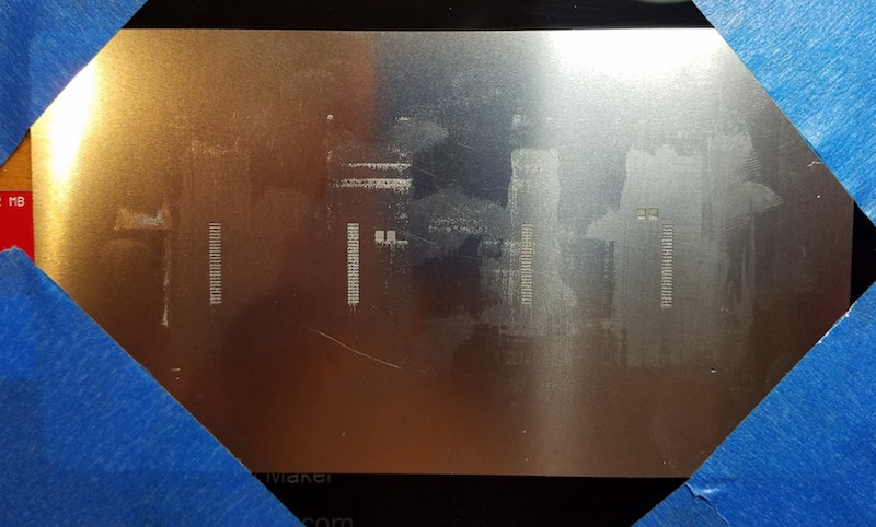
In my previous attempt, I used purpose-made plastic framing pieces to hold the PCB while I applied solder paste with the stencil. These plastic pieces were a tiny bit thicker than the PCB, resulting in the stencil floating above the surface of the PCB instead of resting on it. The amount of float was less than 0.3 mm, but it was still enough to cause problems. This time I used extra PCBs to create a frame, so the thickness was an exact match with no float. The solder paste application looked pretty much spot-on, as you can see here:
Placement of the chips is still difficult. I’m doing it by hand with a pair of tweezers, and the best I can do is to drop the chip within a couple of millimeters of the correct position. Then I slide it around until it’s in the right spot, smearing a bit of the solder paste in the process. Here’s how things looked after chip placement:
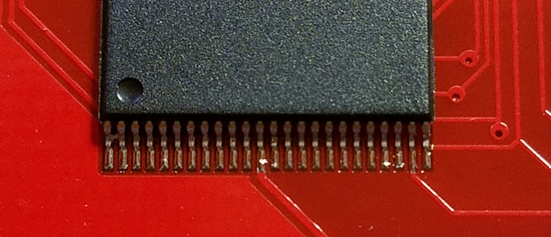
After reflow on my hot plate, the results were pretty good, but unfortunately there were still several solder bridges. Here’s a typical example. It all looks decent, except for those two pins at the far left. The chip also didn’t snap to the correct alignment, as I’d been led to believe would happen thanks to the surface tension of liquid solder. The alignment is pretty good, but not quite centered, and there’s a bridge at pin 1:
I assembled ten boards this way, with two chips per board, and two sides to be soldered per chip, making a total of 40 sides. The good news was that 14 of the 40 sides had zero solder bridges. The bad news was that about half the sides had 2+ solder bridges, and I never assembled a PCB that didn’t have at least one solder bridge on it somewhere. This was the final score:
0 solder bridges: 14 sides
1 solder bridge: 7 sides
2 solder bridges: 7 sides
3 solder bridges: 3 sides
4+ solder bridges: 9 sides
I discovered that I needed to wipe both sides of the stencil clean after each use, otherwise the solder paste application grew progressively messier with each new PCB. I also found that I wasted a lot of solder paste. Dispensing the minimum possible amount from my syringe was still too much, and resulted in a lot of leftover paste on my plastic scraping tool. It was hard to reuse the paste stuck to the scraper. When I tried it a couple of times, using another scraper to clean off the first scraper, the results weren’t good.
End?
Is this the end of my reflow soldering saga? I think so, at least for this particular PCB. I don’t think I can improve further on these results without more effort than can be justified, yet the speed and quality of the process isn’t good enough to replace my current method of drag-soldering with an iron. I’ll revisit this again the next time I have a new PCB to assemble, and I’ll try to stay away from 0.5 mm pitch parts in my designs.
Read 7 comments and join the conversationReflow Soldering with Hot Plate and Stencil
This was my 5th attempt to assemble some ROM-inator II boards using reflow soldering, instead of my normal drag-soldering with an iron. After various failures in the previous attempts, this time I used a stainless steel stencil to apply solder paste to the pads, hoping the stencil was the missing ingredient needed for success. I’ll save you the suspense: it didn’t work any better than my earlier efforts. I think I’m cursed.
You can read about the previous reflow attempts here:
1. Reflow with hot air
2. Switched to a hot plate
3. With an aluminum pie pan
4. New solder paste and aluminum sheet
The ROM-inator II PCB has two chips with 0.5mm pin spacing, which makes home reflow particularly challenging. If my boards only had larger components, SOICs, and the like, my attempts would probably have gone much better. With the 0.5mm chips, no matter what method I tried, I ended up with numerous solder bridges between adjacent pins. I was able to fix up the solder bridges manually with an iron, so all the boards worked in the end, but reflow totally failed as a faster and easier replacement for drag-soldering. For that, I’d need boards to come out of reflow with zero solder bridges at least 80-90% of the time, and I was never anywhere close to that level of success.
Stencil Process
I ordered a 4 mil stainless steel stencil from OSH Stencils, and paid a little over $20 for the stencil and a couple of acrylic framing pieces. Ordering was easy, but I did run into a a few problems with my paste layer generated by EAGLE. The paste layer also contained my board outline, which I clearly didn’t want cut into the stencil. It also contained openings for all the edge contact pads on the PCB, which are not meant to be soldered. It required some extended futzing around in EAGLE in order to suppress the unwanted outline and pads, and generate a new paste file.
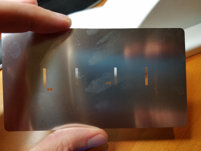
I taped the acrylic framing pieces to my desk, along with an extra blank PCB, to create a secure frame. Next, I placed a ROM-inator II PCB in the frame, and taped the stencil over it. Aligning the stencil correctly with the pads underneath was easier than I expected, even for the sub-millimeter sized pads. I then squirted some solder paste from a syringe onto the stencil, and used a plastic card to scrape the paste across the stencil, filling the holes.
Framed area for PCB:
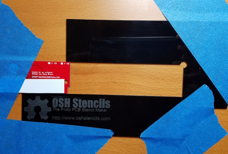
Blank PCB in frame:
Stencil positioned on top of PCB:
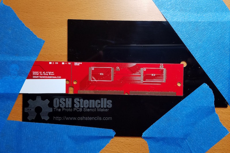
Solder paste applied to the stencil:
After scraping paste across the stencil:
The PCB after removing the stencil:
Scraping the paste into the stencil openings was more difficult than I’d expected. I’d thought I would be able to make a single pass and fill all the holes, but some holes only partially filled with paste, even when there was plenty of paste scraped over them. Something to do with the thickness of the stencil, the size of the openings, or the viscosity of paste maybe? I had to make repeated passes from different directions with the plastic scraper before all the stencil openings were filled evenly.
One problem I hadn’t anticipated was the thickness of the acrylic framing pieces. They’re about 1.5mm thick, but the ROM-inator II PCB is only 1.2mm thick, resulting in the stencil floating 0.3mm above the PCB. 0.3mm may not sound like a lot, but it’s about 3x the thickness of stencil. In practice, the stencil flexed enough that it mostly sat flush on top of the PCB, but it clearly wasn’t ideal.
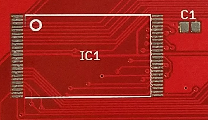
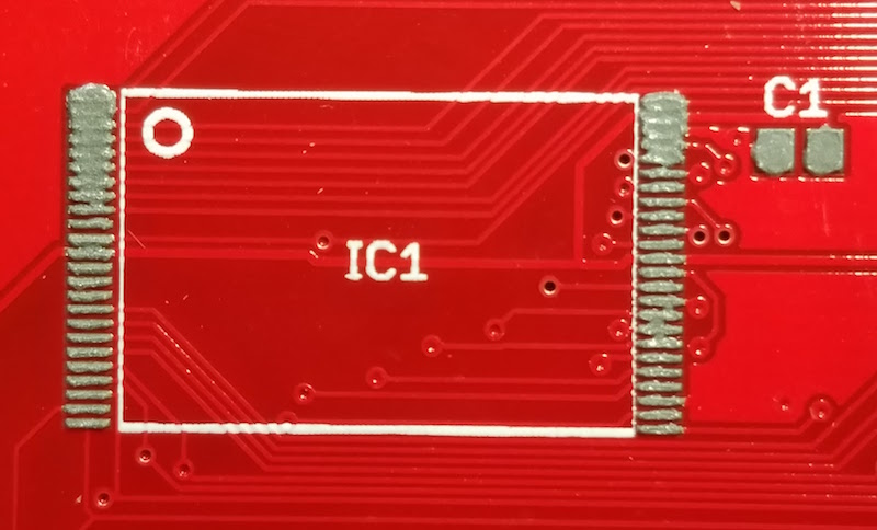
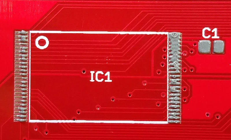
The final photo above shows the mixed results of solder paste application. For larger things like the C1 capacitor, it was great. And for many of the individual pads on chip IC1, there was a nice clear line of paste right on the pad. But for many other pads, the solder paste was smeared between several adjacent pads. Not good.
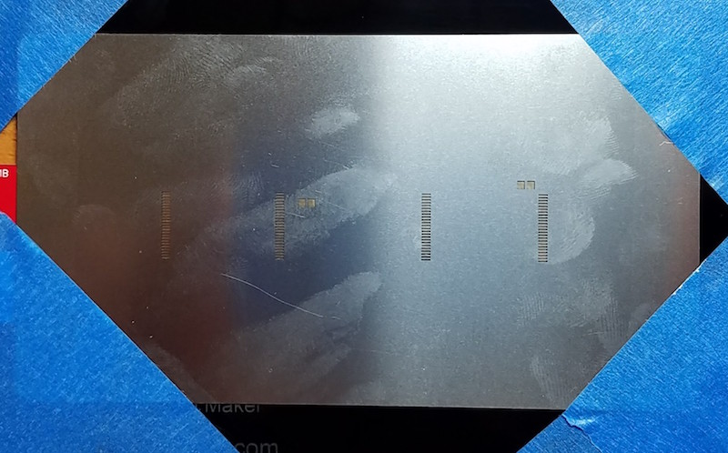
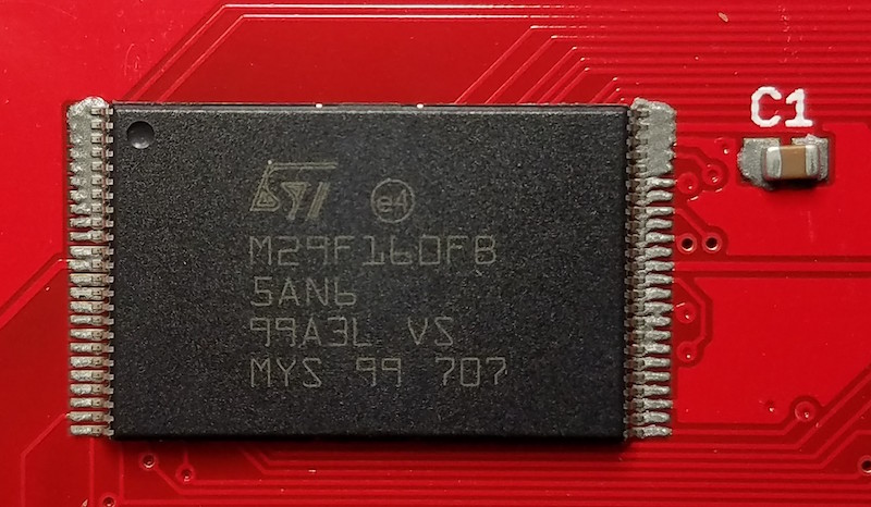
The final difficulty was placing the chip on the pads. Even where I had clean lines of paste, it was difficult to position the chip accurately without smearing the paste around in the process. I would drop the chip down with tweezers, close to where it needed to go, but “close” wasn’t close enough. Even a tiny sub-millimeter nudge to line up the chip properly was enough to smear paste from one pad to the next, possibly negating the whole benefit of using a stencil in the first place. Here’s what things looked like after placing the chip, but before reflow:
Results
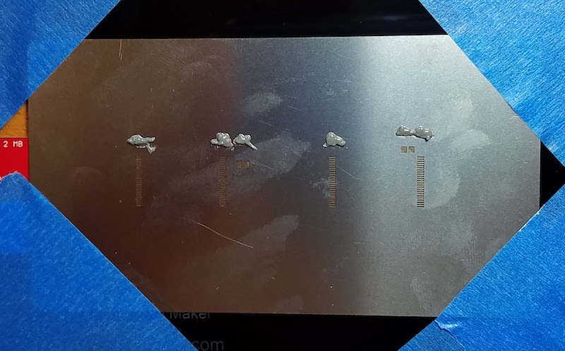
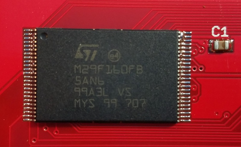
The result was similar to all my previous attempts: lots of solder bridges. Not surprisingly, most of the bridges showed up in those areas where the solder paste was smeared before reflow, but some bridges appeared even in areas where the paste had looked OK. Here’s how the same chip looked, after reflow with the hot plate:
I tried a second PCB, this time attempting to use less solder paste overall, but the results were the same. Then I tried a third PCB, and scraped the solder paste across the stencil left-to-right, parallel to the orientation of the pads, instead of perpendicular. That resulted in some weirdly uneven application, and more of the same solder bridges after reflow.
I could never get the solder paste application to come out cleanly, and it always seemed like too much.
Conclusions
At this point I’ve run out of blank ROM-inator II PCBs, so my experiments will have to stop for a while. I hate to end a series on a down note, but I’m a little frustrated and disappointed with this whole effort. Maybe I would get better results with thinner frame pieces, or a toaster oven instead of a hot plate, or yet another brand of solder paste, or a different paste applicator, or more flux, or a pick-and-place, or… but at some point I have to admit this just isn’t working. Once I get more blank PCBs to play with, I’ll consider whether to try further experiments.
Read 8 comments and join the conversation