

Reflow Soldering with Hot Plate and Stencil
This was my 5th attempt to assemble some ROM-inator II boards using reflow soldering, instead of my normal drag-soldering with an iron. After various failures in the previous attempts, this time I used a stainless steel stencil to apply solder paste to the pads, hoping the stencil was the missing ingredient needed for success. I’ll save you the suspense: it didn’t work any better than my earlier efforts. I think I’m cursed.
You can read about the previous reflow attempts here:
1. Reflow with hot air
2. Switched to a hot plate
3. With an aluminum pie pan
4. New solder paste and aluminum sheet
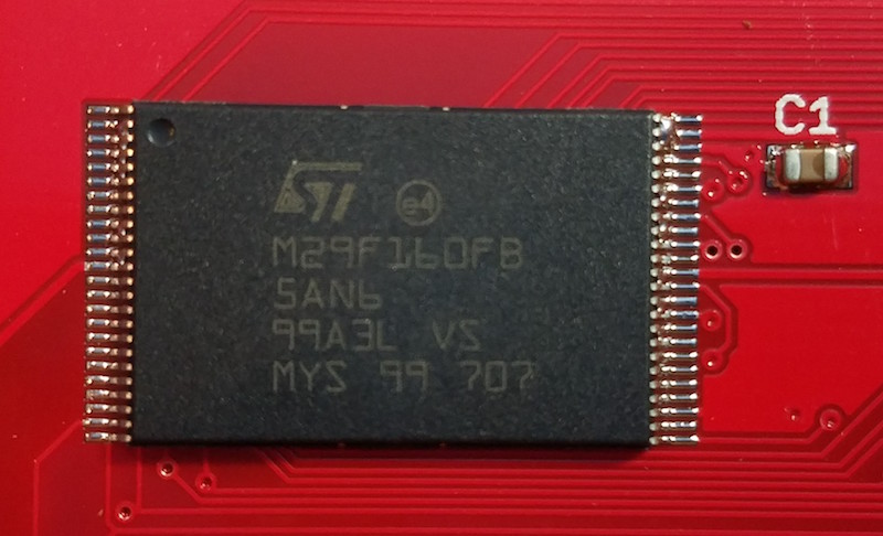
The ROM-inator II PCB has two chips with 0.5mm pin spacing, which makes home reflow particularly challenging. If my boards only had larger components, SOICs, and the like, my attempts would probably have gone much better. With the 0.5mm chips, no matter what method I tried, I ended up with numerous solder bridges between adjacent pins. I was able to fix up the solder bridges manually with an iron, so all the boards worked in the end, but reflow totally failed as a faster and easier replacement for drag-soldering. For that, I’d need boards to come out of reflow with zero solder bridges at least 80-90% of the time, and I was never anywhere close to that level of success.
Stencil Process
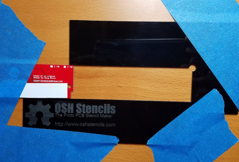
I ordered a 4 mil stainless steel stencil from OSH Stencils, and paid a little over $20 for the stencil and a couple of acrylic framing pieces. Ordering was easy, but I did run into a a few problems with my paste layer generated by EAGLE. The paste layer also contained my board outline, which I clearly didn’t want cut into the stencil. It also contained openings for all the edge contact pads on the PCB, which are not meant to be soldered. It required some extended futzing around in EAGLE in order to suppress the unwanted outline and pads, and generate a new paste file.
I taped the acrylic framing pieces to my desk, along with an extra blank PCB, to create a secure frame. Next, I placed a ROM-inator II PCB in the frame, and taped the stencil over it. Aligning the stencil correctly with the pads underneath was easier than I expected, even for the sub-millimeter sized pads. I then squirted some solder paste from a syringe onto the stencil, and used a plastic card to scrape the paste across the stencil, filling the holes.
Framed area for PCB:
Blank PCB in frame:
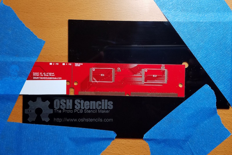
Stencil positioned on top of PCB:
Solder paste applied to the stencil:
After scraping paste across the stencil:
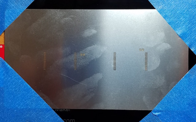
The PCB after removing the stencil:
Scraping the paste into the stencil openings was more difficult than I’d expected. I’d thought I would be able to make a single pass and fill all the holes, but some holes only partially filled with paste, even when there was plenty of paste scraped over them. Something to do with the thickness of the stencil, the size of the openings, or the viscosity of paste maybe? I had to make repeated passes from different directions with the plastic scraper before all the stencil openings were filled evenly.
One problem I hadn’t anticipated was the thickness of the acrylic framing pieces. They’re about 1.5mm thick, but the ROM-inator II PCB is only 1.2mm thick, resulting in the stencil floating 0.3mm above the PCB. 0.3mm may not sound like a lot, but it’s about 3x the thickness of stencil. In practice, the stencil flexed enough that it mostly sat flush on top of the PCB, but it clearly wasn’t ideal.
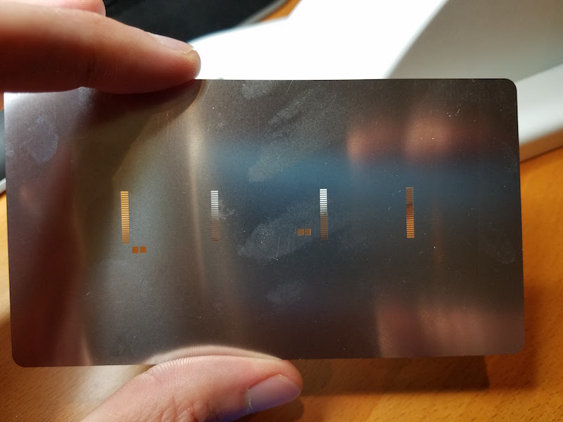
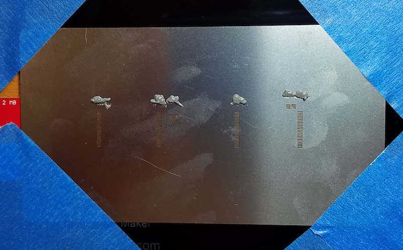
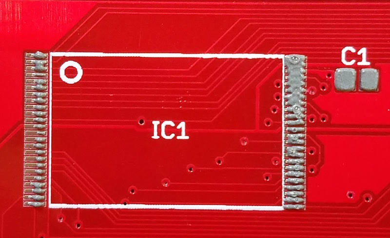
The final photo above shows the mixed results of solder paste application. For larger things like the C1 capacitor, it was great. And for many of the individual pads on chip IC1, there was a nice clear line of paste right on the pad. But for many other pads, the solder paste was smeared between several adjacent pads. Not good.
The final difficulty was placing the chip on the pads. Even where I had clean lines of paste, it was difficult to position the chip accurately without smearing the paste around in the process. I would drop the chip down with tweezers, close to where it needed to go, but “close” wasn’t close enough. Even a tiny sub-millimeter nudge to line up the chip properly was enough to smear paste from one pad to the next, possibly negating the whole benefit of using a stencil in the first place. Here’s what things looked like after placing the chip, but before reflow:
Results
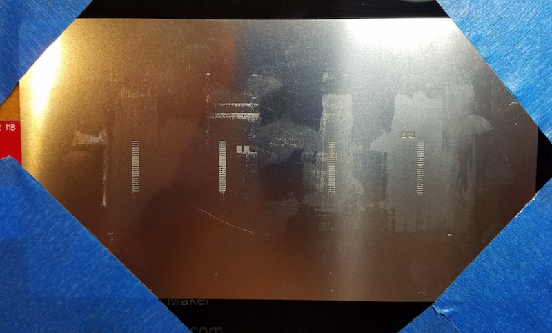
The result was similar to all my previous attempts: lots of solder bridges. Not surprisingly, most of the bridges showed up in those areas where the solder paste was smeared before reflow, but some bridges appeared even in areas where the paste had looked OK. Here’s how the same chip looked, after reflow with the hot plate:
I tried a second PCB, this time attempting to use less solder paste overall, but the results were the same. Then I tried a third PCB, and scraped the solder paste across the stencil left-to-right, parallel to the orientation of the pads, instead of perpendicular. That resulted in some weirdly uneven application, and more of the same solder bridges after reflow.
I could never get the solder paste application to come out cleanly, and it always seemed like too much.
Conclusions
At this point I’ve run out of blank ROM-inator II PCBs, so my experiments will have to stop for a while. I hate to end a series on a down note, but I’m a little frustrated and disappointed with this whole effort. Maybe I would get better results with thinner frame pieces, or a toaster oven instead of a hot plate, or yet another brand of solder paste, or a different paste applicator, or more flux, or a pick-and-place, or… but at some point I have to admit this just isn’t working. Once I get more blank PCBs to play with, I’ll consider whether to try further experiments.
Read 8 comments and join the conversation8 Comments so far
Leave a reply. For customer support issues, please use the Customer Support link instead of writing comments.
There should not be extra paste between pads after lifting the stencil, as seen in your images. You should only tape one side of the stencil. Then spread away from the tape. Optimally this can be done in a single pass (you need to apply the right amount of pressure at the correct angle), but as you’ve discovered, it takes practice.
You’re putting down too much paste. It’s hard to tell from the photos, but it looks like the paste is the same size as the pads. The paste should not cover the entire pad, but be shrunk slightly relative to the pad size. You might need to adjust your pad footprint as well if it’s not working for you.
Thanks. In retrospect, the too-thick frame pieces probably caused most of the problems I had here. They caused the stencil to float slightly above the PCB, so it took more solder paste to fill the cavity below, and there was opportunity for bleed-through underneath. Tellingly, the solder paste application was worse near the top of IC1 than near the bottom, even when I wiped the paste on from left to right. The top of IC1 is the area closest to the edge, where the size of the gap under the stencil would be largest.
The openings in the stencil appear to be the exact same size as the pads underneath – it’s whatever EAGLE did as a default. If I ever do another stencil, I could look at making them smaller than the pad.
Should I be worried about throwing clean-up paper towels in the household trash? I used them to wipe the stencil and applicator clean, so they have a small amount of solder paste on them, which contains lead. I guess people throw much worse stuff in the trash all the time (dead batteries, junked electronics), but I want to do the right thing.
It’s not perfect, but the solder joints are getting there. The whole pad is wetted and the pins are centered.
If you don’t have a frame of the right thicknessyou can just use spare PCBs. Just fix 3 of them to you work surface with tape.
As has been said before, spreading the paste requires some practice. If it doesn’t look right after paste application, wipe it off and repeat the process. For spreading I would recommend a putty knive. If possible, buy one wider than your row of pads. That way you can hit them all with ine single swipe. Maybe also buy some fine-grid sand paper and grind the edge of the putty knive so it’s smooth and even.
Hey Steve!
I think you should slap some flux on the boards before using the reflow oven
That might just do the job
Boo– I really wanted this to work for you! Are you going to give up? (Hope not…)
Steve,
Your problem is clearly excessive paste on the pcb. As stated earlier, the quick fix is to use an extra pair of the pcbs you wish to stencil to form an “L” shape guide on the bench. Just make sure you secure the alignment pcbs with tape on the outer edge and outer corners using thin tape so as not to lift the stencil away from the pcb surface. This should provide the exact depth you need for accurate paste dispensing.
Over the years I have used all sorts of stencils and your absolute best bet is with stainless steel between 0.10 and 0.12 mm thickness for the fine pitch components. I work a lot with UFQFPN (no lead) 0.500 mm pitch and rarely have issues.
The long term solution within eagle is to load up the component library, select each pad and uncheck the cream layer. You can then go back and manually “draw” a narrow cream layer using the rectangle tool. This method gives you much finer control over the opening dimensions that will be transferred your stencil.
If you are still having issues I would be happy to reflow a hand full of boards for you with your existing stencils and pcbs. Can’t be *that* difficult. :\
These PCBs with bridges are fairly easy to fix, and having a bridge or two is par for the course. Flood the area with flux, use some very fine solder braid soaked in flux and gently touch the edge of (while hot) to a pair of pads… fixed. It takes some practice. The trick to hand rework (for me anyway) is flux. Lots of it, because it encourages things bead up and the bridges to naturally separate with surface tension.
As others have said also, that is way way too much solder paste. I just do these sorts of packages by hand, only using paste and oven or hot air with BGAs (or sometimes QFN).
Cheers,
J.
Easiest way to adjust for the too thick frame is to put some masking tape down in the PCB cavity to raise the PCB up to flush with the top of the frame.
For placing the chips – https://blog.ohmnilabs.com/diy-vacuum-pickup-smt-pick-and-place