

More AVR ICSP Footprints
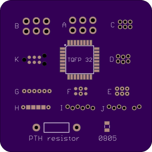
I’m continuing to research options for alternative programming headers for AVR microcontrollers, building on the ideas I discussed earlier. For one-time programming purposes, the standard 3 x 2 pin 0.1 inch header is just… too big. I’m on the hunt for something that’s smaller, and that can be used on a bare footprint without actually soldering a header. The mockup above shows a 1.5 x 1.5 inch board with the options I’m considering, along with size references from a 32-pin AVR, an 0805 resistor, and a through-hole resistor.
A – The standard 3 x 2 footprint for 0.1 inch pin header.
B – 3 x 2 pin 0.1 inch footprint with zig-zag or lock hole spacing. This helps temporarily hold a header in place through friction.
C – 3 x 2 footprint for 0.05 inch pin header. It’s a lot smaller, but the hole spacing is tiny.
D – 3 x 2 pin footprint with zig-zag spacing for 0.05 inch pin header.
E – 3 x 2 pin footprint for pogo pins with 0.05 inch spacing. It’s nearly the same as C, except the drill holes are smaller. It’s designed for something like the Pogo Key, where the tips of pogo pins snap into the holes, but unlike C the pins don’t actually pass through the holes.
F – An alternative footprint for E. Two positions are holes to help align and stabilize the Pogo Key, and the other four positions are one-sided pads, so more of the PCB’s bottom side is available for other traces and components.
G – 6 x 1 pin footprint for pogo pins with 0.05 inch spacing, inspired by the Pogo ISP Micro. It’s essentially a Pogo Key with a linear layout instead of rectangular.
H – An alternative footprint for G. Two positions are holes to help align and stabilize the pogo pin adapter, and the other four positions are one-sided pads, so more of the PCB’s bottom side is available for other traces and components.
I – 6 x 1 pin footprint with zig-zag spacing for 0.05 inch pin header. Example
J – An alternative footprint for I. The six pins are split into groups of four and two, to prevent backwards insertion of the header.
K – Tag-Connect 6-pin no-legs version.
Here’s a look at the bottom side of the board. No surprises here, but just a visual reminder that the footprints using pads leave more empty space on the bottom for other purposes than the footprints using holes.
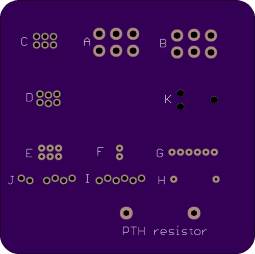
Is using pads better than using holes? I’m not sure. Pads leave the PCB’s bottom more open, but the signal routing for pads may require extra vias for switching between layers that wouldn’t be needed for holes, so it’s not a clear win. Holes also provide something for pogo pins to grip, and are the only way to use 0.05 inch header pins.
Is 0.05 inch spacing clearly better than 0.1 inch spacing? The footprints based on 0.05 inch spacing are obviously smaller, but the holes/pads are so closely spaced that there’s no room to squeeze a trace between them. The larger 0.1 inch spaced footprint is permeable to unrelated signal routing, so although it’s large, it’s not always a major impediment to board layout. The 0.05 inch spaced footprints are like walls that blocks all other signal traces.
I also see a risk of accidentally shorting neighboring holes/pads with the 0.05 inch spaced footprints. The copper of one is only about 10 mils away from its neighbor. If the programmer pins are slightly misaligned as they are lowered onto the board, a pin could land in the empty space between two holes/pads and cause a brief short circuit.
Are 6 x 1 linear footprints better than 3 x 2 rectangular ones? This is hard to answer. They’re the same total area. My first intuition was that 6 x 1 would be easier to fit into otherwise wasted space around the edges of the board. But after looking at it visually, I have an easier time imagining tucking that 3 x 2 into an unused spot than the 6 x 1.
And a Word About Tag Connect
Several people replied to my earlier post to say they’re happily using the Tag Connect cable. From what I’ve read elsewhere, they seem to have a loyal following. Its footprint K is arguably among the best of the options shown here. Yet I’ve almost totally ruled out the Tag Connect, for a reason that you might find silly.
The problem I have with Tag Connect is that it’s a cable and a pogo pin holder combined into a single unit. It’s designed to replace the existing cable on your AVR programmer, rather than attach to the end of the cable as with the other options discussed here. That means you have to purchase different versions of the Tag Connect cable depending on what programmer you have – one version fits the AVR ISP mkII, another fits the Atmel ICE, etc. If you’ve got a USBasp programmer, you’re out of luck, or will have to design your own adapter.
I own both an AVR ISP mkII and an Atmel ICE, so in theory I’d need to buy two different Tag Connect cables. If I wanted to have something assembled and programmed by a third party, I’d also have to worry about what model of programmer they have and whether a Tag Connect cable exists for it. The result would be a lot of hassle and equipment duplication, compared to any of the other options, where I could just snap an adapter onto the end of the existing programming cable.
Perhaps I could design my own adapter board for the generic Tag Connect cable, so any programmer’s 3 x 2 pin female header could plug into my adapter, and Tag Connect’s 3 x 2 pin female header could plug into another socket on the adapter. But this would result in twice the total cable length, which might impact signal quality and reduce the maximum possible bit rate for programming. Edit: I see that Tag Connect sells an adapter board like this for other MCUs, so maybe it’s fine and signal degradation isn’t a problem.
If Tag Connect sold something similar to the Pogo Key but with alignment pins, it would be a great option. But as things stand with the integrated cable, it complicates programming for anybody with multiple different programmers or who contracts third party programming with unknown programmer hardware.
Read 9 comments and join the conversation9 Comments so far
Leave a reply. For customer support issues, please use the Customer Support link instead of writing comments.
Can’t you use an edge connector like a PCI card and plug the entire board into a socket like you get on pc motherboards for expansion cards for programming ?
Wouldn’t an edge connector require much more space than any of the other alternatives? Even if you’re only using a few edge pads for signals, you’d still need to reserve the entire length of the board. Any other components or pads near the edge would prevent the board from fitting in the socket, or would short out in the socket.
Why would you need to reserve the whole edge? Just use a six-position edge connector. You could use something like this connector in a custom cable: https://www.digikey.com/product-detail/en/phoenix-contact/1893724/277-8990-ND/3605477
The connector is keyed (you need a slot between particular pads on the PCB) so you can’t connect it wrong.
You’re right – an open sided socket wouldn’t require reserving the whole edge. That clamp connector is interesting, although I’m not sure what the advantage would be over any of the alternatives discussed here. I suppose it clamps more securely than the other options? But the required board area is much bigger than even the 0.1 inch header footprint I have now. I don’t think it would work with curved edge PCBs like my Star Ring either.
On PIC16F1xxx parts, the cable length limit that microchip states (6 inches) is crap. It was a few years ago when I did it, but I was able to program with well over 3 feet of cable. You couldn\’t debug, but that\’s because the ICD firmware had a read-modify-write problem.
If you put a little R-C termination on your adapter board, that would go a long way to make the signal cleaner if you need it.
Hi,
The Pogo Key and Pogo ISP Micro designs look great but I wonder if it’s possible to do a little better. For example, take footprint H.
By offsetting the power pin from the line it would key the mechanism and make it difficult to insert backwards. The programming adaptors that you link to have settled on soldering the length of the pogo pin along the length of a PCB. If the power pin was soldered to the other side of the PCB then it would easily and accurately implement the appropriate keying. If manufactured on suitably thick board it might even be possible to offset the pin by an entire pin’s width and make it even safer.
It might also be able to make the footprint smaller on the underside of the board by making the first and third pins the ones with the holes and the rest of them pads. Hopefully one of the pins with the holes can be the one that’s offset from the rest for a bit of added stability. Your point about vias is interesting. Perhaps it’s possible to choose which side of the board to put the header on or perhaps that’s another trade-off against ease of access during manufacturing?
All good points. Yes a keyed version of H would be nice, either with an offset pin like you describe, or with a 4+2 arrangement similar to J.
But I am realizing belatedly that all the footprints expect Tag Connect have a fundamental flaw: there’s a risk of wrong connections and possible circuit damage when connecting the programmer to a powered-on board. They all involve bringing live pins (pogo pins or standard male header pins) in contact with the board, then sliding the pins around until they line up with the pads/holes. For instance J prevents you from fully inserting the pins incorrectly, but it doesn’t prevent the pins from making contact with the annular ring for the wrong holes.
You can’t use extra-long pogo pins as guide pins either, as I’d anticipated for G and H. Sure you could mount the outermost pogo pins so they stick out further than the others, and assign signals to those two pins that are safe when misconnected. But pogo pins compress. With a little pressure, the outer pins will compress and the inner pins will make board contact, potentially in the wrong place.
Basically you can’t safely use a signal pin as a guide pin. The only safe solution is to use non-conductive guide pins, like Tag Connect, or like the keyed edge connector that tim1724 mentioned. I could add longer non-compressible non-conductive guide pins to the other footprints, but I’m starting to think I should just go with the Tag Connect instead of trying to reinvent the wheel. My main objection to TC was the cable, but it sounds like that can be solved with a single inline adapter and the extra cable length isn’t a problem.
It is not necessary to keep all the ISP pins in a cluster. To save space and make layout easier, you can place the pads wherever they fit best on the board. You can then make a very cheap and simple programming jig out of a PCB and some pogo pins that can end up having a faster programming cycle time than any normal ISP footprint.
Here is an example where I really needed the space on a small and very low spec board. You can see the iterations the jig went though (with input from the line workers using it) to be very very fast….
Photos and files:
https://github.com/bigjosh/Vibe-V2/tree/master/programming%20jigs
Video:
https://www.youtube.com/watch?feature=player_embedded&v=tlA72ofPwDw
Some notes:
1. Depending on the AVR and if the board has power, you likely do not need all 6 pins. No need to place and contact pins that are not used.
2. Holes are not necessary, but I’ve found that conical pins into holes are nice because they are self aligning and there it a large contact area so better connection.
3. With a little more work, you can make the programming cycle start automatically when the board touches down on the contacts by sensing the current through the pins. This can speed up programming significantly since if frees up both of the operators hands.
LMK if any questions!
-josh
Do you have any recommendations on solutions for adding direct USB firmware updating to an AVR project? I’d like to allow ordinary end-users to not be required to have a programmer to apply firmware updates to my device. Would be nice to just connect micro usb and run a program to update the firmware.