Archive for the 'Yellowstone' Category
Current Limiting Strategies (Again)
I’ve returned to the question of how best to limit the current from Yellowstone’s -12V supply. I discussed this earlier here and here, and had more-or-less settled on the idea of using a current mirror circuit. But now I’m taking a second look at possibly using JFETs or a purpose-designed CCR (constant current regulator) intended for powering LEDs instead.
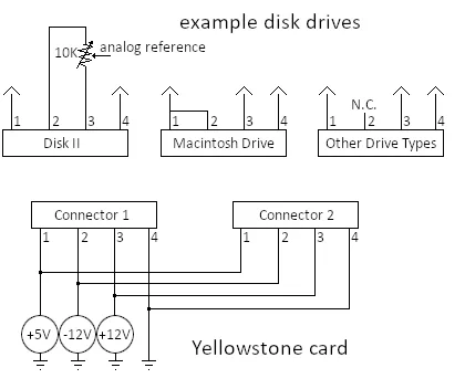
Here’s a review of why this is needed. Yellowstone has two connectors for disk drives, and each drive is supplied with +5V, +12V, -12V, and GND. Some types of drives don’t actually use the -12V supply, and other types have the -12V supply pin internally connected to the +5V supply pin. Ouch! A picture may help clarify:

The idea is to insert some new component or circuit inline with pin 2 (the -12V supply pin) of each Yellowstone drive connector to prevent a short circuit when a Macintosh drive is connected. Keeping in mind there might be two Disk IIs connected, or two Mac drives, or one of each, or any combination with other drive types. The anti-short-circuit protection should happen automatically, without requiring any user switch settings or other manual configuration.
Ideally the solution would just disconnect pin 2 when a Macintosh drive is connected, but I don’t know any good way to do that. The next best solution is to limit the current through pin 2, to a level that’s high enough for a Disk II to operate normally, but low enough to prevent problems with the Macintosh drive.
Here are the requirements for the -12V supply connection, as I see them:
- When a Disk II drive is connected, it should see a supply voltage as close to -12.0V as possible, since it uses the supply in an analog reference circuit. This means any resistors between the drive and Yellowstone’s -12V supply should be small, to minimize the voltage drop.
- When a Macintosh drive is connected, the current should be limited to about 10 mA. The exact value isn’t critical, and anything from 5 mA to 20 mA is probably OK.
- The two drive connectors should be isolated from one another, so a Mac drive at connector 1 doesn’t affect the -12V supply for a Disk II drive at connector 2.
- The current limiting function should work automatically, without any control or reset logic.
- Power dissipation in the current limiter should be as low as possible.
- The current limiter should be built from commonly-available parts.
- The current limiter should use the fewest possible number of parts, that are small and inexpensive.
Current Mirror
In my last post, I considered using a current mirror. In this circuit, a reference current is passed through a transistor, with two other transistors controlling the -12V supply current, one transistor per drive connector. It can be built with three matched BJTs or FETs, plus a single resistor for setting the current limit.
Here’s an example using FETs, with a Disk II drive plugged into the first connector and a Mac drive plugged into the second. The -12V supply current is shown for each drive connector. The current for the Disk II is nearly identical to the 2.4 mA that would be expected if no current-limiting circuit were present. But the current for the Mac drive is limited to 9.5 mA, instead of the many amps that would otherwise flow due to the short circuit.

A current mirror requires each transistor to have the same voltage threshold, gain, temperature, and other properties, else the current may be incorrect. This is where my difficulties begin. I went looking for a single IC package with 3 FETs, or maybe 4 FETs, in order to help ensure they’d all have matching properties. I learned that these aren’t common: you can find discrete FETs or dual FET packages, but beyond that it’s slim pickings. With the global shortage of semiconductors, I’d prefer not to rely on a part whose availability might be an issue in the future.
I could easily use two dual FET packages, or three discrete FETs, but then their temperatures and other properties might not be well matched. Given that I can tolerate an error of least 2x in the current, maybe this isn’t a big worry. I need to take a closer look at the FET datasheets to get an idea of how much the current might change if one transistor’s threshold voltage is 0.1V off from another’s, or one’s temperature is at 25C and the other is at 85C. Maybe it’s not a big enough issue to worry about for this application.
One small drawback of the current mirror is that it wastes 10 mA from the -12V supply to create the reference current, regardless of whether any of the connected drives actually use the -12V supply.
JFET
Another approach to current limiting is to use a self-biased JFET. A commenter on one of my previous posts mentioned this option, but I never followed up on it. The basic idea is that a JFET is a “default on” device, but its drain-source channel can be partially closed by making the JFET’s gate-to-source voltage negative. The more negative you make Vgs, the further the channel is closed, until reaching the Vgs cutoff threshold where the JFET turns off completely. By adding a resistor at the JFET’s source terminal, and connecting it back to the gate, this behavior can be leveraged to make a current limiter. There’s a nice tutorial about this here.

The JFET’s IDSS (its maximum drain-to-source saturation current) must be larger than the desired current limit. If the circuit can’t reach the current limit, because there’s a large external resistance like in the case of the Disk II drive, the behavior is less obvious to me. From my scrutiny of graphs in the datasheets, it looks like a typical JFET in this situation will behave like a resistor of about 80 ohms, in series with the external resistor used to set the current limit.
Yellowstone would use two independent JFETs for the two disk connectors, with no reference current needed or wasted. That’s nice.
The higher “on” resistance compared to a normal FET is less nice. Combined with the external resistor, it would create a larger voltage drop, so the Disk II drive would see a voltage like -11.7V instead of -12.0V. Maybe that’s still fine. I did a test earlier with a Disk II and a 100 ohm series resistor on the -12V supply, and it seemed to work OK.
It’s slightly complex to calculate what value of external resistor is needed to achieve a desired current limit. The formula depends on the current, the JFET’s IDSS, and its cut-off voltage. The tutorial linked above has the derivation. Or you can eyeball it from the graphs in the datasheet, if a precise value isn’t needed.
I couldn’t find many widely-available dual-JFET packages, which is too bad. So a Yellowstone solution using JFETs would probably be built with two discrete JFETs and two resistors, to make a separate current limiter for each drive connector.
Constant Current Regulators

The JFET sounds intriguing, but then I stumbled across the concept of constant current regulators. From what I can tell, these CCRs are just the JFET plus resistor circuit described above, all wrapped up into a two terminal package that looks like a diode. CCRs are available in different types with different fixed current limits, and are typically used in LED driving applications. As far as I can tell, their behavior is identical to the JFET circuit with the discrete resistor.
Since a CCR is a two-terminal device, it would be very easy to use: just put one in series between the drive and the -12V supply for each drive connector. Boom, done. It’s too easy, I think I must be missing something.
This specific NSI50010YT1G CCR from ON Semiconductor looks nearly perfect, with a built-in current limit of 10 mA. The trouble is that right now it’s unavailable just about anywhere. There’s a 15 mA version in stock at Newark, but that’s still only a single supplier, and I’d rather have 10 mA than 15. I really like the idea of using a CCR, but it’s not going to work unless I can find one with an appropriate current limit, with good availability from multiple suppliers.
Power Dissipation
For any of the above solutions, when a Macintosh drive is connected and the current is limited to about 10 mA, the power dissipation must be considered. With +5V at the Mac drive end and -12V at the Yellowstone end, that’s 17V times 10 mA, or 170 mW of power. Most of the packages that I looked at have power dissipation limits close to that, or slightly higher. I’m uncertain how to optimize this, but probably I need to choose packages that are physically bigger (violating my requirement 7), and/or make the PCB pads very large so they can double as heat sinks. These kinds of power considerations are mostly foreign to me. I don’t want to make the PCB pads any larger than absolutely necessary, since board space is at a premium in the area near the -12V connections. If anyone has recommendations for package types or connection methods that would be better for dissipating a few hundred milliwatts, I’d love to hear them.
And the Winner Is…
I’ll do some more searching for CCR availability. If I can find one with the right properties and that’s widely available, I think that’s my preferred solution.
Otherwise I’ll probably stick with the original plan of using a current mirror and three FETs. I can build it with two dual FET packages plus a single resistor, leaving me with an extra FET available for some future purpose. I’ll do some more analysis and testing to try to estimate how much current error I might see if the reference current FET is in a different package than the FET that limits the current. As long as the answer is closer to 20 percent than 400 percent, it should be OK.
Read 17 comments and join the conversationFPGA In-System Programming: Beginnings

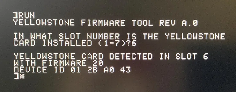
I’ve written several times about Yellowstone’s need for in-system FPGA reprogramming. Once the Yellowstone card is in the user’s hands, the user needs a way to update the FPGA firmware when new versions are released, without requiring a JTAG programmer or some kind of USB interface built into the card. The current Yellowstone prototype was designed to support in-system FPGA programming, but it had never been tested until today. The photo here shows a BASIC program on an Apple IIe successfully communicating with the FPGA’s SysConfig port and reading its device ID. I’ve verified that 01 2B A0 43 is the expected ID for the Lattice MachXO2-1200HC FPGA on the Yellowstone board, so everything looks correct. It will still be a long road from here to reach the point where the FPGA is actually reprogrammed, but this proves that the basic communication mechanism works, which was the part I was most concerned about.
Yellowstone’s in-system programming support doesn’t require any extra hardware on the board, which is great! It’s all implemented through PCB routing, connecting the right signals to the right pins. The MachXO2 FPGA supports communication with its built-in SysConfig hardware through many different interfaces including JTAG, I2C, and a Wishbone interface implemented in the FPGA logic, but I’ve chosen to use the SPI interface. This is a “hard” SPI port, so reconfiguration and reprogramming via SPI should work even if the FPGA is in a fubared state or is completely blank.
How do you connect the Apple II peripheral bus to the SPI port, in a way that avoids accidental transitions on the SPI I/O signals, but allows for full bidirectional SPI I/O when needed? Here’s how I did it.
CS: The SPI SysConfig port has a chip select input pin, which is normally high, leaving the SPI port disabled. As long as CS remains high, it doesn’t matter what’s happening on the other SPI I/O signals, and the FPGA will ignore it. The CS input is connected to another FPGA pin that’s normally in a Hi-Z state, but that can be driven low by FPGA logic. This makes it possible to programmatically enable the SPI port by having the Apple II CPU write a magic value to a special address, which the FPGA logic watches for, in order to drive CS low. For situations where the FPGA is blank or in a bad state, the programmatic enable may not work. In this case there’s also a hardware jumper on the PCB that can be used to force CS low.
DI: The data input is address line A0.
CLK: The SPI clock is the Apple II /DEVSEL signal. This means an SPI data bit will be clocked into the FPGA from A0 whenever there’s a low-to-high transition on /DEVSEL. This signal is normally high, but it goes low for about 500 ns whenever the Apple II CPU makes a memory reference to the “device” region of the peripheral card’s memory. For Yellowstone, this region is where the virtual IWM lives, in address range $C0E0 to $C0EF (assuming the card is in slot 6).
DO: The data output from the SPI port is connected to another FPGA input pin. Yellowstone’s FPGA logic includes a special behavior that makes use of this. If the SPI port is enabled and the CPU reads from address $C0EA or $C0EB, the FPGA will return the SPI DO bit that it sampled on its other pin, rather than the normal return value from the IWM.
If this last piece sounds somewhat complicated, it is. The DO bit needs to get on the data bus somehow, so that the CPU can read it. But DO can’t be directly connected to the 5V data bus – it must connect somewhere on the 3.3V side in the Yellowstone logic, and then the ‘245 bus driver must be enabled at the proper time to drive the DO value onto the 5V bus. The ‘245 enable timing is under control of the FPGA logic. That means when the FPGA is blank or in a bad state, there’s no ‘245 enable, so there’s no way for the CPU to read DO. In short, a correctly-configured FPGA is a requirement for reading DO. Without this, the program running on the Apple II will need to proceed with blind SPI communication in which it can send data but not receive it. Fortunately this seems to be sufficient to perform FPGA reprogramming. I don’t see any way around this inability to read DO when the FPGA is blank without adding extra hardware to Yellowstone, which I’m loathe to do for such a rare situation. So be it.
When all of this is put together, the SPI communication looks like this: The CPU writes a magic value to a special address to force CS low. Then it begins a series of reads from $C0EA or $C0EB. Every read from $C0EA transmits a 0 bit because A0 is 0, and every read from $C0EB transmits a 1 bit. In either case, D7 of the byte that’s read is the reply bit from the SPI port. The rest is all software to transmit the correct bit sequences and make sense of the replies.
Now onward to the FPGA datasheet, where I can learn what sorts of magic SPI incantations are required to actually reprogram this thing.
Read 10 comments and join the conversationYellowstone Option Configuration Design
The Yellowstone disk controller’s whole reason for existence is its ability to control any type of Apple II disk drive, but for a few Apple II programs, this universality causes problems. Yellowstone handles standard 5.25 inch drives just fine, but some software gets confused when it doesn’t find the ROM for a standard Disk II Interface Card in slot 6. For these rare cases, Yellowstone has an option to enable a “compatibility mode” where it emulates a plain vanilla Disk II Interface Card without any extra bells and whistles. The question is how does the user enable compatibility mode?
In the current version of the Yellowstone prototype, the choice is determined by a DIP switch. But as I’ve been refining the design, I’ve developed a strong dislike of DIP switches. They’re big and awkward, and not at all user-friendly. I’ve already managed to find ways to eliminate two of the four DIP switches on the board, and if I can find another solution for enabling compatibility mode then I can eliminate a third DIP switch.
My first thought was to check the keyboard immediately after the computer is powered-on, before loading anything from the disk. If the ‘C’ key is held down (c for compatibility), I could enable compatibility mode, otherwise I could proceed normally. On the Apple II it’s easy to check for keypresses by examining memory address $C000. If there’s a keypress waiting, the MSB will be 1 and the lower seven bits will hold the ASCII value of the key. So I could check for the value $C3 ($80 plus $43) and everything would be peachy.
Unfortunately, I quickly discovered that one of the first things the Apple II ROM does after a reset is to clear the keyboard buffer. This happens before control is transferred to Yellowstone’s ROM, so by the time my code checks the keyboard buffer, it’s too late. What to do?
Rely on the Buffer’s Lower Bits
From testing on my Apple IIe, the keyboard buffer isn’t actually zeroed when it’s “cleared”. The MSB is set to 0, but the other seven bits still retain the ASCII value of the key. So perhaps my code could just check $C000 for $43 instead of $C3 to detect the ‘C’ key, and it would work as originally intended.
This seems slightly dubious, since I’m not sure if this is documented behavior, or if other models of Apple II will clear the keyboard buffer in the same way. There’s also a small bug this introduces: if ‘C’ was the last key typed, and you then turn off the computer and turn it on again within 1-2 seconds, $C000 will still hold the value $43 during power-up. This may lead to accidentally detecting non-existent keypresses and enabling compatibility mode when the user didn’t intend to.
Delay Booting and Poll the Buffer
Another option is for Yellowstone to sit in a busy loop after the computer is first powered-on, and continuously poll the keyboard buffer looking for the value $C3. If the keyboard has a key repeat behavior, then $C3 will appear in the buffer after roughly 0.75 seconds if the ‘C’ key is continuously held down. Or the user could be instructed to quickly tap-tap-tap the ‘C’ key when the computer is powered-on, instead of holding it continuously down. This would eliminate any dependency on the keyboard’s key repeat behavior. At least one modern Apple II peripheral card uses this method.
The main drawback of this approach is that it would introduce a busy-waiting delay every time the computer is turned on. To reliably detect a key repeat or a tap-tap-tap, Yellowstone would need to insert a startup delay of about one second, every time the computer powers-on or resets. It sounds like a small thing, but I think I’d find this delay very annoying. Furthermore, the key repeat behavior might not work on the original Apple II or Apple II+ keyboard, so tap-tap-tap is probably the only reliable solution.
Check the Open Apple Key
A third alternative is to check whether the Open Apple key is held down, instead of the ‘C’ key or any other standard key. The behavior of the Open Apple key is very different from the other keys. Open Apple is just a duplicate of the first button on the first game controller, and its current status can be read at memory address $C061. As long as Open Apple is held down, the MSB of $C061 will be 1.
The Closed Apple key works identically, and its state can be read at address $C062. But holding the Closed Apple key during power-up will trigger the Apple II’s built-in diagnostics, so that key isn’t a good candidate for triggering Yellowstone behavior changes.
For now I’ve implemented Yellowstone’s compatibility mode enable using the Open Apple key, and it works well on my Apple IIe. Unfortunately, earlier models of Apple II computers don’t have an Open Apple or Closed Apple key. Users with those computers would need to attach a game controller and press its button during power-on, which is far from ideal. There’s also a risk that some other third-party peripheral cards might use Open Apple in the same way, which would make it impossible to trigger Yellowstone’s compatibility mode without also affecting the other card. But I don’t know of any specific cards that use Open Apple, so maybe I shouldn’t be concerned.
Something Else
I could stick with the DIP switch, despite its awkwardness. Or I could ask users to perform some voodoo in the Apple II monitor, and write a magic value to a special address in the card’s memory to enable compatibility mode. Or some other solution I haven’t thought of yet. Opinions?
Read 27 comments and join the conversationYellowstone and Macintosh Floppy Drives
Testing continues for my Yellowstone disk controller card for Apple II computers. One of the design goals for Yellowstone was to support Macintosh floppy drives, and today I got a Mac drive working for the first time! I transplanted a 1.44 MB high density internal floppy drive from a Macintosh LC, and successfully used it to boot an Apple IIe with an 800K ProDOS disk. Hooray!
Some more details: The 1.44 MB Macintosh drive can be used to read 800K Apple II disks. Yellowstone does not support 1.44 MB disks. While I haven’t tried it yet, an 800K Macintosh drive should work too. 400K Macintosh drives will not work, but 400K disks in 800K or 1.44 MB drives should work. Clearly there will need to be substantial testing for all this.
So far, so good. But there was some cheating involved in this test, related to differences in pin assignments between Apple II and Macintosh floppy drives. Now I need to determine how to make everything work for real.
RD and SENSE Pin Usage
The first issue involves how the drive sends information to the computer. The Sony 3.5 inch drive mechanism sends all its disk data and status info on a single pin: RD, pin 16 of the 20-pin rectangular connector. But for reasons I don’t understand the Apple II software is designed to expect 3.5 inch disk data on the RD pin but status info on pin 20. If you look inside the Apple 3.5 Drive enclosure, you’ll find an adapter board that (among other functions) copies the value from RD onto pin 20 also. But when direct-connecting a Sony 3.5 inch drive mechanism without an enclosure, there’s no adapter, and the Apple II gets confused.
For this test, I was able to get things working by modifying the FPGA logic to use pin 16 instead of pin 20 when looking for status info, but this breaks the 5.25 inch and Smartport disk modes. I need to find some auto-magic way of doing this only when necessary.
-12V Supply Connection
The second issue is with the -12V power supply for the drive. Somewhere over the years and the generations of Apple II and Macintosh computers, Apple changed the meaning of pin 9 of the 20-pin rectangular floppy drive connector. On Apple II computers and disk controllers, and on the earliest Macs, this pin is -12V. But on later Macintosh models, pin 9 is not connected at the disk controller side. On the drive side (at least with the 1.44 MB drive I pulled from my Macintosh LC) pin 9 is a redundant 5V power supply connection, and -12V isn’t used. That means using a 20-pin ribbon cable to plug a Macintosh 3.5 inch drive directly into the Yellowstone card will create a short circuit between -12V and +5V. Ouch!
I avoided this short-circuit by physically cutting the wire for pin 9 on my disk cable, but that’s not an acceptable long-term solution. I could add a -12V enable jumper to the Yellowstone card, and that would work, but it would still leave the possibility of accidental -12 to +5V short circuits if somebody made a mistake or didn’t read the instructions. A better solution would somehow detect what kind of drive was connected, and automatically enable or disable -12V accordingly.
How might that work? Why do some drives need -12V anyway? As far as I know, the only drives that actually need the -12V supply input are 5.25 inch drives like the Disk II. From a quick look at the Disk II schematic, -12V appears to be part of a 10K ohm potentiometer circuit, with +12V on the other side of the pot. Maybe this is the pot used to adjust the disk rotation speed? I’m not sure.
Whether pin 9 is a -12V supply input, or is a second +5V pin (with the primary +5V supply on pin 11), the direction of current flow will be from the drive to the disk controller. So I can’t solve this problem with a simple diode. Maybe there’s something clever I can do here with a transistor? If the pin is supposed to be a -12V supply input, but the Yellowstone board hasn’t (yet) provided the necessary -12V, then I’m not sure what voltage will be sensed at the pin. My guess is it will be +12V, as seen through that 10K pot. Based on this, I don’t see any easy and reliable method of auto-detection, so maybe a -12V jumper is the only viable solution.
Read 22 comments and join the conversationYellowstone Glitch, Part 10: Resolution?
Good news! I’ve completed the stress test involving seven filled peripheral slots to increase the data bus capacitance to its maximum, and Yellowstone is still performing OK. I tried this stress test on both the Apple IIgs and Apple IIe, with Yellowstone connected to an Apple 3.5 Drive, Unidisk 3.5, or Apple 5.25 Drive. With more peripheral cards and more bus capacitance, this test should produce the highest currents through Yellowstone’s 74LVC245 bus driver chip. If the card were ever going to malfunction due to high currents, ground bounce, or similar electrical problems, this test should have revealed it.
Despite all the various hardware modifications that I tried, the resolution was ultimately implemented entirely with FPGA logic changes designed to minimize current and avoid simultaneously switching current. Here’s the complex dance that happens now when the CPU reads a byte from Yellowstone’s RAM:
- t=0: IOSTROBE is asserted by the Apple II. The FPGA puts the value 10101010 on the input pins of the ‘245 bus driver, but the ‘245 is not yet enabled.
- t=140ns: The ‘245 bus driver gets enabled. This 140 ns delay avoids a period of bus-fighting due to the slow-turn around time of the motherboard’s data bus driver. The value 10101010 is driven onto the data bus.
- t=210ns: The FPGA disables its output pins, and enables the RAM. The actual RAM value is now driven onto the data bus.
- t=350ns: RAM gets disabled. Now nothing is driving the ‘245 inputs, but the FPGA’s keeper circuitry maintains the last value from RAM. This early RAM shutoff separates the change in supply current from further changes happening at the next step.
- t=420ns: The ‘245 bus driver gets disabled. Now nothing is driving the data bus, but bus capacitance maintains the last-driven value.
- t=490ns: (or t=630ns for long clock cycles) IOSTROBE is deasserted and the bus cycle ends.
So is this saga all done? Everything good? End of story? Not exactly.
Even though it may not be absolutely necessary, I’m going to replace the 74LVC245 bus driver with a 74LVCR2245. This is a drop-in replacement with integrated 26 ohm series resistors on the outputs to limit the current. Thanks to LIV2 for making me aware of this option. I’ll sleep better at night with the 74LVCR2245 replacement. Its only real drawbacks are that it increases the BOM count and cost slightly, and it’s not exactly the most common chip, so availability might become a problem in the future. But if that happens I can just switch back to 74LVC245 without needing any PCB modifications.
Now that I’ve opened this can of worms on signal integrity, I find it mentally difficult to close it again. My design has mainly focused on correctness of the digital logic, with little thought given to the low-level world of currents and voltages that implement the digital abstraction. Now I see that many of my design practices were not very good, and I want to improve them. I already needed to design a Yellowstone 2.1 PCB to fix an overlapping signal trace, and I’m including several other changes in 2.1 as well:
- widened all the power and ground traces as much as possible
- improved the ground fills, addressing some choke points and connecting dead-end areas
- spread out some signal traces that were unnecessarily crowded
- added a 0.1uF capacitor across 5V and GND at the card’s supply pins (there was already a 10uF here)
- moved the 0.1uF capacitor on the 3.3V regulator output to be closer to the regulator
- moved all the decoupling capacitors to be close to the chips’ VCC pins instead of their GND pins
- rerouted the data bus traces so they don’t all cross under the A0-A6 address traces
I’m not sure whether rerouting the data bus traces was really necessary. But if there’s a total instantaneous current through all eight data traces of 250 to 500 mA, with a sharp change in current, and all eight of the data traces pass under an address trace on the opposite side of a 2-layer board, is that enough to induce a glitch in the address? Maybe? If so, rerouting those traces should help.
In hindsight I’m not sure whether it was wise to move decoupling capacitors to be adjacent to VCC pins instead of GND pins. Most advice that I’ve read says to place them as close as possible to the supply pins, meaning both power and ground. But on a chip where the VCC and GND pins are in opposite corners, it’s a direct tradeoff: the closer the capacitor is to the VCC pin, the further it is from GND. Faced with this choice, is one location better than another?
My first thought was that it doesn’t matter, and what’s important is minimizing the total combined trace length from the capacitor to the VCC and GND pins. This makes some intuitive sense. But then I did some more reading, and I think capacitors close to the GND pin may actually be more effective at reducing ground bounce, while capacitors close to the VCC pin may be more effective at reducing VCC sag.
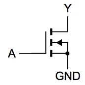
Consider the case of an open drain buffer, which at its simplest could just be a single transistor with its source connected to ground, its gate connected to the input signal, and its drain connected to the output. When the input is high, it will pull the output low, and when the input is low, the output floats:

A buffer like this would be susceptible to ground bounce, but there’s no VCC here at all. So what good would it do to locate a capacitor close to the buffer’s VCC pin, if it even had one? To minimize ground bounce, it seems to me that the capacitor should be located close to the ground pin, with the other terminal connected to any other supply source, which doesn’t necessarily need to be the VCC pin. But I’m having some difficulty imagining the current flows in this example, and maybe my reasoning is wrong.
I’ll keep tinkering with this stuff in the background, but now I can finally return to functional testing of Yellowstone and addressing high-level firmware bugs. It’s progress.
Read 8 comments and join the conversationYellowstone Glitch, Part 9: Scope Probe Ground Leads

The role of Steve will now be played by a small red-faced boy
Oops. I’ve verified that the spikes I’m seeing on data signals are largely due to the embarrassingly poor ground connections on my oscilloscope probes, rather than issues with the signals themselves. I had the ground leads of all four scope probes clipped together, connected to a 12 inch wire, which was then plugged into a ground point on the Apple IIgs motherboard, which was about 8 inches away from the peripheral slot where the Yellowstone card was installed. That’s a very long return path. I hadn’t appreciated how important it is to have a good short ground lead connection for the scope probe when measuring signals with fast edges, even though nice people kept trying to explain it to me. Now I have some new data using better ground connections.
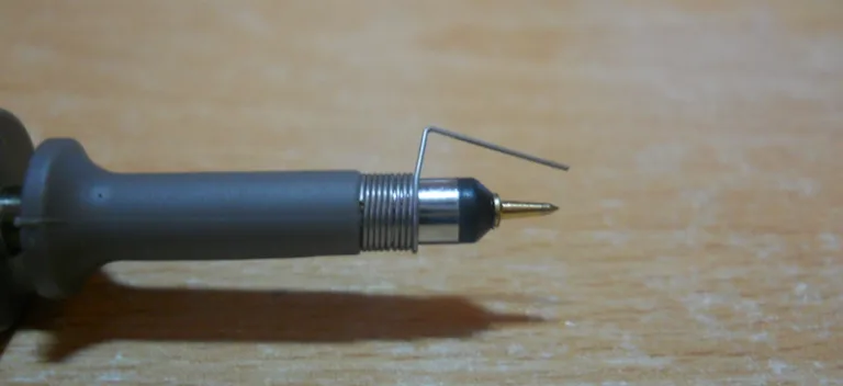
To begin, I removed the spring hook adapter from the probe, and also detached its standard ground lead (a 4 inch wire with an alligator clip). This left me with a sharp-tipped spike probe. Then I wrapped a small ground spring around the outside of the probe. This was included with my bag of oscilloscope parts, but I’d never used it before. The end result looked similar to the photo above. Now I was ready to take some new measurements.
To review, here’s another look at the scope capture from part 7, with the old bad probe grounding. This was the example where I captured signals from an unpopulated PCB, when the Yellowstone card was not installed in the computer. Yellow (Ch1) is the 5V supply voltage, measured at the 5V pin of the PCB. Notice how there are spikes of more than 1V peak-to-peak in the 5V supply.

Now here’s the same experiment again, but with the probe tip for 5V directly touching the 5V pin, and the ground spring touching an adjacent GND point a few millimeters away. The probes for the other signals were still connected in the old way.

Wow! The spikes on the 5V supply completely disappeared with this more careful measurement. But I quickly discovered that it’s very difficult to accurately position a spike probe and a ground spring in a live circuit. While taking these measurements I managed to accidentally short 5V and GND not once but twice. One of the episodes produced sparks. Yikes.
Next I reinstalled the Yellowstone card, and repeated some of my earlier measurements, but with a better ground setup. It wasn’t practical to use the spike probe and ground spring here, but I did the best I could. I hooked a short piece of wire to a ground point on the Yellowstone board, and connected the standard ground leads from all four probes to this wire. Here’s what I saw:
- Blue (Ch4) is address line A1. It’s a 5V input from the Apple II
- Purple (Ch3) is data bus D0 from the Apple II
- Yellow (Ch1) is the 3.3V supply voltage, measured at the VCC pin of the ‘245.
- Cyan (Ch2) is IOSTROBE from the Apple II, and marks the boundaries of the bus cycle.

Now I could see some supply noise again (yellow channel), but it looked fairly minor. Also some modest ringing on the data bus D0, though probably not enough to worry about. Unfortunately I still observed lots of spikes on A1 (dark blue channel). It appeared that whenever the data bus value changed (pink channel), it created spikes on A1. This was true regardless of whether Yellowstone was driving the data bus, during the low period of IOSTROBE (cyan channel), or if something else was driving the data bus, during the high period of IOSTROBE.
That degree of spikes on A1 looked concerning – possibly enough to cause a malfunction if the scope were showing a true representation of the signal. To get a better look, I needed a better ground lead for the probe. So I soldered a tiny coiled wire to the A1 pin to use as an anchor for the probe, and went back to my spike plus ground coil setup. Then I veeeery carefully applied the probe and took a measurement, without any sparks. This time I didn’t capture D0 or 3.3V, and A1 was on Yellow Ch1:

It’s harder to understand what’s happening here without the D0 trace for reference. There’s still some spiking on A1 during the bus cycle when IOSTROBE is low. This is the moment when Yellowstone’s 245 is enabled and driving the data bus. But the amplitude of the spikes during the bus cycle looks much smaller than before, only reaching about 400 mV at worst. That should probably be OK.
There’s worse spikes on A1 when its value changes, after the bus cycle ends, but I don’t think I can do anything about that since Yellowstone is inactive at this time.
Using the same probe setup, I took some other measurements of A1 (not shown) outside of Yellowstone bus cycles, during times when the data bus value changes due to something else driving the bus. I observed similar spikes of about +/- 300mV on A1 whenever the data bus changed. I’m not sure what’s causing that, but it seems to be unrelated to anything that Yellowstone is doing.
TLDNR
In short, after taking better measurements with better probe grounding, all the signals looked decently OK.
Given this, it’s probably time to try the stress test: fill all the peripheral slots with 1980s vintage cards, which should increase the bus capacitance to its maximum, which in turn should produce the highest currents through Yellowstone’s 245 bus driver chip. It shouldn’t really matter what those other cards are or what they’re doing, the only important thing is that they’re installed. If Yellowstone is ever going to fail due to high currents, ground bounce, or similar electrical problems, this should reveal it.
For this test I’ll use a new Yellowstone board with the normal chips, instead of the Frankenstein board with which I’ve been experimenting up until now, that’s been modified too many times to count. I’ll use the updated FPGA logic with pre-driving 10101010 and other changes I’ve made to help reduce peak current, but otherwise it will be identical to the board whose mysterious IIgs failures originally launched this whole glitching saga. If this test reveals any problems, I’ll look more into adding series resistors. Otherwise I’ll move on.
Read 2 comments and join the conversation