

Yellowstone Glitch, Part 10: Resolution?
Good news! I’ve completed the stress test involving seven filled peripheral slots to increase the data bus capacitance to its maximum, and Yellowstone is still performing OK. I tried this stress test on both the Apple IIgs and Apple IIe, with Yellowstone connected to an Apple 3.5 Drive, Unidisk 3.5, or Apple 5.25 Drive. With more peripheral cards and more bus capacitance, this test should produce the highest currents through Yellowstone’s 74LVC245 bus driver chip. If the card were ever going to malfunction due to high currents, ground bounce, or similar electrical problems, this test should have revealed it.
Despite all the various hardware modifications that I tried, the resolution was ultimately implemented entirely with FPGA logic changes designed to minimize current and avoid simultaneously switching current. Here’s the complex dance that happens now when the CPU reads a byte from Yellowstone’s RAM:
- t=0: IOSTROBE is asserted by the Apple II. The FPGA puts the value 10101010 on the input pins of the ‘245 bus driver, but the ‘245 is not yet enabled.
- t=140ns: The ‘245 bus driver gets enabled. This 140 ns delay avoids a period of bus-fighting due to the slow-turn around time of the motherboard’s data bus driver. The value 10101010 is driven onto the data bus.
- t=210ns: The FPGA disables its output pins, and enables the RAM. The actual RAM value is now driven onto the data bus.
- t=350ns: RAM gets disabled. Now nothing is driving the ‘245 inputs, but the FPGA’s keeper circuitry maintains the last value from RAM. This early RAM shutoff separates the change in supply current from further changes happening at the next step.
- t=420ns: The ‘245 bus driver gets disabled. Now nothing is driving the data bus, but bus capacitance maintains the last-driven value.
- t=490ns: (or t=630ns for long clock cycles) IOSTROBE is deasserted and the bus cycle ends.
So is this saga all done? Everything good? End of story? Not exactly.
Even though it may not be absolutely necessary, I’m going to replace the 74LVC245 bus driver with a 74LVCR2245. This is a drop-in replacement with integrated 26 ohm series resistors on the outputs to limit the current. Thanks to LIV2 for making me aware of this option. I’ll sleep better at night with the 74LVCR2245 replacement. Its only real drawbacks are that it increases the BOM count and cost slightly, and it’s not exactly the most common chip, so availability might become a problem in the future. But if that happens I can just switch back to 74LVC245 without needing any PCB modifications.
Now that I’ve opened this can of worms on signal integrity, I find it mentally difficult to close it again. My design has mainly focused on correctness of the digital logic, with little thought given to the low-level world of currents and voltages that implement the digital abstraction. Now I see that many of my design practices were not very good, and I want to improve them. I already needed to design a Yellowstone 2.1 PCB to fix an overlapping signal trace, and I’m including several other changes in 2.1 as well:
- widened all the power and ground traces as much as possible
- improved the ground fills, addressing some choke points and connecting dead-end areas
- spread out some signal traces that were unnecessarily crowded
- added a 0.1uF capacitor across 5V and GND at the card’s supply pins (there was already a 10uF here)
- moved the 0.1uF capacitor on the 3.3V regulator output to be closer to the regulator
- moved all the decoupling capacitors to be close to the chips’ VCC pins instead of their GND pins
- rerouted the data bus traces so they don’t all cross under the A0-A6 address traces
I’m not sure whether rerouting the data bus traces was really necessary. But if there’s a total instantaneous current through all eight data traces of 250 to 500 mA, with a sharp change in current, and all eight of the data traces pass under an address trace on the opposite side of a 2-layer board, is that enough to induce a glitch in the address? Maybe? If so, rerouting those traces should help.
In hindsight I’m not sure whether it was wise to move decoupling capacitors to be adjacent to VCC pins instead of GND pins. Most advice that I’ve read says to place them as close as possible to the supply pins, meaning both power and ground. But on a chip where the VCC and GND pins are in opposite corners, it’s a direct tradeoff: the closer the capacitor is to the VCC pin, the further it is from GND. Faced with this choice, is one location better than another?
My first thought was that it doesn’t matter, and what’s important is minimizing the total combined trace length from the capacitor to the VCC and GND pins. This makes some intuitive sense. But then I did some more reading, and I think capacitors close to the GND pin may actually be more effective at reducing ground bounce, while capacitors close to the VCC pin may be more effective at reducing VCC sag.
Consider the case of an open drain buffer, which at its simplest could just be a single transistor with its source connected to ground, its gate connected to the input signal, and its drain connected to the output. When the input is high, it will pull the output low, and when the input is low, the output floats:
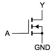
A buffer like this would be susceptible to ground bounce, but there’s no VCC here at all. So what good would it do to locate a capacitor close to the buffer’s VCC pin, if it even had one? To minimize ground bounce, it seems to me that the capacitor should be located close to the ground pin, with the other terminal connected to any other supply source, which doesn’t necessarily need to be the VCC pin. But I’m having some difficulty imagining the current flows in this example, and maybe my reasoning is wrong.
I’ll keep tinkering with this stuff in the background, but now I can finally return to functional testing of Yellowstone and addressing high-level firmware bugs. It’s progress.
Read 8 comments and join the conversation8 Comments so far
Leave a reply. For customer support issues, please use the Customer Support link instead of writing comments.
“I’m going to replace the 74LVC245 bus driver with a 74LVCR2245. This is a drop-in replacement with integrated 26 ohm series resistors on the outputs to limit the current. […] availability might become a problem in the future. But if that happens I can just switch back to 74LVC245 without needing any PCB modifications.”
Why? An eight-resistor SMD array is dirt cheap, needs just a few pads on that large PCB, and is a real no-brainer. Bus on one side, peripheral on the other side. Done. No hard-to-find parts needed.
That’s true. The advantage of the 74LVCR2245 is avoiding layout changes stemming from repositioning the 74LVC245 to make space for a separate resistor array.
http://www.1000bit.it/support/manuali/apple/technotes/iigs/tn.iigs.068.html
This link may be helpful. Not sure I sent it.
I’m also looking at 74AHC245 as an alternative to 74LVC245 or 74LVCR2245. AHC is very similar to the LVC family, with 5V tolerant inputs, but it’s a slower chip with lower current drive: only 4 mA compared to 24 mA for LVC. That should cut down on ground bounce and ringing quite a bit. It’s better and cheaper and more widely available than LVCR. The only drawback is some loss of noise margin: the Vih is 2.3V for AHC compared to 2.0V for LVC and LVCR.
I think the link posted by keith has at least two very helpful paragraphs, quoted here in full:
“Ground Noise
Since the Apple II expansion slots were designed with only one ground pin, complex expansion cards sometimes have problems with excessive ground noise — especially in the IIGS, where the signals typically have faster rise and fall times. To reduce ground noise as much as possible, it is helpful to bypass all four supply voltages (+5 volt, +12 volt, -5 volt, -12 volt) to ground with electrolytic or solid tantalum capacitors, even if all the available voltages are not used on the expansion card. This additional bypassing has the effect of providing an improved ground by providing additional AC ground paths through the various supply pins.
To maintain a consistent ground quality over the board area on two-layer boards, it is important to properly grid the Vcc and ground traces and to fill in unused areas with ground plane.”
The extra capacitors should be easy to implement, don’t cost much, and if they don’t help or in the worst case cause more problems, you can simply omit them from the PCB.
Also, I recommend to view EEVblog videos 859 and 1085 about bypass capacitors. Hint: You want more than one per supply line.
Good suggestions. I’d been wondering if bypassing the other power supplies might help with ground bounce, even if Yellowstone doesn’t use those supplies. It’s nice to see it confirmed in the Apple tech note.
A bypass cap on e.g. the -5V supply would be like a bypass cap connecting the card ground to the main board’s ground, but with the main board’s capacitance and the traces connecting it in series with the added cap. If the Apple’s motherboard has 0.1uF caps bypassing each supply right next to the connector, then adding a 0.1uF cap on -5, -12, and +12 would be roughly equivalent to adding three 0.05uF caps to the motherboard grounds. If the motherboard only has one bypass cap for each supply rail, located in the middle of the expansion cards, then a card in slot #4 might receive about as much benefit from the bypass caps as it would if the main board had a bypass cap next to every card, but a card in slot #1 or slot #7 would likely receive far less benefit. I’m not sure which description better fits any particular Apple models.
You may have seen this. Found this looking for something else. And the point is moot. Mostly
Cheers