

68000 Interleaved Memory Controller Design
Continuing my efforts on the Plus Too Macintosh Plus clone, I’ve started work on the design of the interleaved memory controller. The memory controller allows RAM to be transparently shared between the 68000 CPU and the video circuitry. The general principle of operation is clear, and is described in many articles about the Mac 128K/512K/Plus, as well as discussions of machines like the Amiga and Atari ST that used a similar scheme. The memory controller forces the CPU and video circuitry to take turns accessing the RAM’s address and data busses. The video circuitry is designed to guarantee that it only accesses RAM during its turn. If the CPU attempts to access RAM out of turn, the memory controller forces it to wait.
I’ve tried to find specific implementation details for this scheme, or a circuit schematic of the memory controller for the Mac, but came up empty-handed. Instead I’ll make some educated guesses about how it worked on the 128K/512K/Plus, and design the circuit myself.
CPU Wait
My first unanswered question is the method used to stall the 68000 if it attempts an out-of-turn RAM access. It’s possible the Mac Plus memory controller gated the CPU clock to stall it when needed, or used the /HALT line. It’s also possible that it used the bus request and bus grant lines /BR and /BG to request the bus from the CPU. However, it’s more likely that it used the 68000 /DTACK line to insert CPU wait states, since this is essentially what that line is for. Some discussions of the Amiga memory controller mention that it used /DTACK for a similar purpose, and it seems reasonable that the Mac did too. During a memory bus cycle, the 68000 expects /DTACK to be asserted by the memory to acknowledge a read or write operation, and it waits as long as necessary until receiving that acknowledgement.
Memory Interleave Pattern
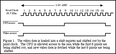
My next question is the exact pattern of interleaved access, and the fraction of time dedicated to the CPU vs the video circuitry. Details are very hard to come by, but it appears that the Plus shared 50/50 between the CPU and video circuitry, with four clock cycles of CPU access followed by four clock cycles of video access. This article at MacTech was the only reference I found, although it shows 16MHz pixel clock cycles instead of 8MHz CPU clock cycles. Here’s their diagram:
Interestingly, the Mac SE seems to have used a 75/25 split, with the CPU having access to RAM 75% of the time, accounting for the SE’s performance edge over the Plus. The Atari ST and Amiga appear to have both used a more aggressive scheme where video circuitry access occurred during known dead time in the 68000 bus cycle, so the CPU never had to wait. This would have required the use of higher speed RAM than found on the Plus or SE, in order to squeeze the video memory access into that timing window. Again, hard details on the memory controller for any of these machines is difficult to find, and this is my interpretation of the many vaguely-worded descriptions I found.
While I could get better performance from my Mac clone by using the ST/Amiga technique, I will use the slower Plus technique to make the clone’s behavior as similar as possible to a real Plus.
68000 Bus Cycle Timing
To really understand how the memory controller can work, it’s necessary to study the 68000 bus cycle timing. The most important point is that all 68000 memory accesses require at least 4 clock cycles. Assuming fast enough memory, they will never require more than 4 clock cycles, so 4 clocks per memory access is the norm. When I first discovered this, I was a bit shocked, since it embeds the “CPU is much faster than RAM” concept directly into the CPU’s design. Even if the RAM were fast enough to perform a read or write in a single clock cycle, the 68000 will still take 4 clock cycles to perform the memory operation. These 4 clock cycles are divided into 8 states named S0 to S7, each half a cycle in length. Here’s a diagram from the 68000 datasheet:
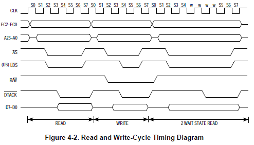
The 68000 sets up the address, strobe, R/W, and data lines (for a write) during states S0 to S3, and expects /DTACK to be asserted at the end of S4. If it’s not, it inserts wait states until /DTACK is asserted, at which point it advances to states S5-S7 to complete the bus cycle. Data is actually latched at the end of S6, and the address and strobe lines are deasserted in S7, to prepare for the next bus cycle.
Memory Controller Design
Note that the 68000’s TAS (test and set) instruction uses a unique 10-clock (20 state) bus cycle that doesn’t fit this pattern. Therefore TAS won’t work using this memory controller. I strongly suspect it didn’t work on the Mac Plus either.
With the 4-clock bus cycle pattern, the necessary structure of a memory controller begins to get clearer. The core is a circuit that delays the assertion of /DTACK if the CPU attempts an out-of-turn RAM access. It also needs a 3-bit counter to count 8 clock cycles and keep track of whose turn it is: the MSB of the counter can serve as the “turn bit”, providing 4 clock cycles each to the CPU and video. A bidirectional bus driver (74XX245 equivalent) will be needed to isolate the CPU and RAM data busses, connecting them only during the CPU’s turn. And a mux will be needed to select between the CPU address and video circuitry address, providing one or the other to RAM depending on the turn bit.
The final detail is the phase relationship between the 3-bit clock counter, and the 68000 bus cycle. If new bus cycles always start when the counter value is 0, then everything will work fine, and the turn bit will change state exactly at the beginning and end of a CPU bus cycle. If they are out of phase, however, bad things could happen, because the turn bit could change in the middle of a bus cycle. This would cause a CPU write to fail, or a CPU read to retrieve garbage. Clearly, some mechanism must force the CPU bus cycles to stay in phase with the cycle counter. There’s some cryptic “read phase” code in the Mac ROM that’s executed very early during the boot process, which I’m sure is related, but damned if I can figure out what it does. There’s a mention of it in this discussion of the Mac 128K.
Putting this all together, here’s my design for a 68000 system containing RAM and ROM and using an interleaved memory controller to share RAM between the CPU and video circuitry. Glorious diagrams courtesy of MS Paint.
First, consider the ROM. Because the CPU is the only component that accesses ROM, the CPU address and data busses can be connected directly to the ROM. All that’s needed is an address decoder to determine whether the current CPU address maps to somewhere in ROM, and generate the ROM chip select signal. A valid memory access will be detected when /AS and one or both of /UDS and /LDS are asserted. This /VALID signal can be connected directly to /DTACK, so the CPU indirectly generates the acknowledge signal itself.
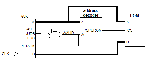
For simplicity this ignores the CPU’s R/W line, and will cause bus contention if you attempt to write to ROM, but the /DTACK behavior is easy to understand.
Now add RAM to the system, along with a linear address generator for video, a video shift register, and other hardware necessary to make it all play nicely together:
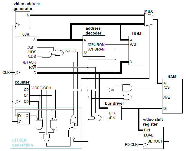
Holy cow, what’s going on here? The CPU address and data busses are still connected directly to the ROM, so that hasn’t changed. /DTACK is now generatred by a more complex circuit outlined in blue, which I’ll return to in a moment.
A three bit counter is incremented every clock cycle, counting a pattern of 8 cycles. When the counter’s MSB Q2 is 0, the CPU may access the RAM, but when Q2 is 1, the video circuitry accesses the RAM and the CPU can’t. A mux selects between the CPU address and video address using Q2 as the selector, with the selected address provided to the RAM. The CPU data bus is isolated from the the RAM’s data lines using a bidirectional bus driver. The bus driver is enabled only when Q2 is 0 and /CPURAM is asserted, meaning it’s the CPU’s turn to access the RAM and RAM is in fact being accessed. The direction of the bus driver is controlled by the CPU’s R/W line.
The RAM is selected whenever Q2 is 1 (it’s the video circuitry’s turn) or /CPURAM is asserted. This means the only time the RAM won’t be selected is when it’s the CPU’s turn, but it’s accessing another memory or peripheral instead of the RAM. The RAM is enabled for writes when it’s the CPU’s turn, /CPURAM is asserted, and the R/W line is 0.
When it’s the video circuitry’s turn, a 16-bit data word from the RAM is loaded into the parallel input of the video shift register. Pixel data for a 1-bit display image is then shifted out the serial output, 1 bit per pixel clock. The pixel clock runs at twice the system clock frequency, and 16 pixels are sent to the display during the 8 system clocks of the three bit counter.
That brings us to the /DTACK generation circuit, which implements the equation:
/DTACK = /VALID + //CPURAM * (/Q2*/Q1 + Q2 + /Q2*Q1*Q0*//LASTDTACK)
Where // indicates negation of a negative logic signal.
So what the heck does that do? Let’s break it down. Whenever this equation results in a value of 1, it means /DTACK will not be asserted, and if the CPU is in state S4 waiting for /DTACK, it will enter a wait state. The equation shows that /DTACK will not be asserted if:
- /VALID is not asserted – No valid address, no acknowledgement. Makes sense.
- Or the CPU is attempting to access the RAM, and any of the following are true:
- Counter value is 0 or 1, indicating the CPU is supposed to be in bus cycle states S0 through S3.
- Counter value is 4 or greater, indicating it’s the video circuitry’s turn, not the CPU’s.
- Counter value is 3 (bus cycle states S6 or S7) and /DTACK was not asserted during the previous clock (bus cycle states S4 and S5)
In the case where the CPU is accessing ROM or another peripheral, the second OR clause drops out, and /DTACK = /VALID as in the earlier ROM-only example. Otherwise /DTACK will be asserted only during the CPU’s turn when the counter equals 2 (CPU should be in bus cycle state S4 and S5), and 3 (S6 and S7) if it was also previously asserted.
If this still doesn’t make sense (I’m not sure I really understand it either), consider what happens when the CPU attempts to access RAM out of turn, and begins a bus cycle when the counter equals 4. It will drive an address (and data, in the case of a write), but since it’s not its turn, the mux and bus driver will prevent the RAM from seeing those values. At the end of the CPU’s state S4, it will expect to see /DTACK asserted, but it won’t be. The CPU will then sit idling through the rest of the video circuitry’s turn, and the first two clocks of its own turn, until /DTACK is finally asserted when the three bit counter reaches 2. The bus cycle will then finish normally, completing exactly at the end of the CPU’s turn.
Phase Again
Lastly, consider what happens if the CPU starts a bus cycle out of phase with the three bit counter. It will expect to see /DTACK asserted at the end of S4, which begins two clock cycles after the start of the bus cycle. That means for a bus cycle starting when the counter equals N, it will expect to see /DTACK asserted when the counter is (N+2) modulo 8.
If the CPU begins a bus cycle when the counter equals:
- 0 – normal case, /DTACK asserted when counter equals 2.
- 1 – CPU will reach state S4 when the counter value is 3. Because /DTACK was not asserted during the previous clock cycle, it will not be asserted now either. The CPU will wait for the remainder of its turn, then all through the video circuitry’s turn, and finally through the first two clocks of its own turn again until the counter equals 2.
- 2,3,4,5 – CPU will reach state S4 during the video circuitry’s turn, and wait for the counter to wrap around back to 2.
- 6,7 – CPU will reach state S4 when the counter equals 0 or 1, which is during its turn, but too early. It will wait until the counter reaches 2 before completing the bus cycle.
No matter when a bus cycle starts, then, it will always finish at the end of the CPU’s turn, keeping the CPU and the three bit counter correctly in phase. The only drawback of a bus cycle that starts out of phase is the additional wait states, which lower the CPU’s average memory throughput. An out of phase bus cycle will likely be attempted at startup, and also whenever two bus cycles are separated by a period of bus inactivity that’s not a multiple of 4 clocks. Fortunately this is uncommon, so normally once the CPU is in phase, it will stay in phase.
Feedback
I would have been thrilled to lift this whole design from some other 68000 system, rather than create it myself, but I couldn’t find one to copy. I’m positive that I’ve made mistakes somewhere, and either overlooked cases where this design won’t work correctly, or where the whole thing could have been accomplished far more simply. Please leave your feedback in the comments, thanks!
Read 7 comments and join the conversation
7 Comments so far
Leave a reply. For customer support issues, please use the Customer Support link instead of writing comments.
“My next question is the exact pattern of interleaved access, and the fraction of time dedicated to the CPU vs the video circuitry”
This is something I believe I have seen info on from some of those Brazillian Mac cloners a couple of years ago. Their Mac clone was slightly faster than the original in some cases because they did this slightly differently. I think there was a tiny bit of extra space in a PAL that enabled a small optimization. Anyway, the guy who did that part of the clone back in the day later wrote about it on a web site.
Indeed! I think you’re referring to this: http://www.merlintec.com/lsi/mac512.html
I sent the author an email asking for his feedback.
Something else to consider in the memory interleaving is that there is a third device needing access to memory as well: the audio output hardware. In the original design I think it picked up a byte during the horizontal blanking interval, so I assume it takes the place of one of the video data fetches. But if you change the timing to be VGA compatible, the sampling time (assuming you stayed compatible with the original sampling rate) might end up during the active video time.
Or are you planning on using the original video timing and not worrying about VGA compatibility?
I will be using VGA 640×480 or 1024×768. That will cause some problems for the audio for sure, unless I can work out something very clever to avoid the problem you mentioned. I haven’t really thought much about the audio yet though…
Yup, that’s the one 🙂
(I think there is or was one other web site that mentioned it but that vague notion is unfortunately all I remember.)
Steve, I only saw your project and these comments today. Since I did the “Turbo Mac” as a consultant, I turned in all material that I produced to Unitron, as well as the schematics they lent me.
Many years later I found out that the very first draft of the equations and report had been forgotten in the back of a drawer. Somebody asked me to scan this material rather than throw it away, and since the project was long dead I didn’t see any harm in doing so.
http://www.merlintec.com/download/unitron1.pdf
http://www.merlintec.com/download/unitron2.pdf
These are huge scanes (8MB or so) of the initial equations for the core PALs with lots of changes and annotations. The few comments and some names are in Portuguese.
http://www.merlintec.com/download/unitronrelatoriop2.pdf
http://www.merlintec.com/download/unitronrelatoriop3.pdf
These are scans of the middle pages of a report on the project. Probably there was some problem while printing and a better version of these two pages was reprinted and sent with the rest of the pages. These are in Portuguese and include some waveforms while a translation of the text to English can be found at:
http://www.merlintec.com/download/unitronreport2and3.txt
A few years ago there was a discussion on comp.arch.fpga about the Mac PALs and someone who had a copy of Apple’s equations posted them. I took a look (they was more complicated than I had expected) but don’t think I saved a copy.
Feel free to email me if you need more details.
[…] covering topics such as the classic Mac’s Crazy Disk Encoding Schemes, the 680000 CPU’s interleaved memory design, various Mac Toolbox Mysteries, an SD Card Floppy Emulator, and […]