

Apple II Card Electrical Woes
The digital abstraction of zeroes and ones is lovely, but electronics debugging often requires a deeper look into the realm of analog signals. That’s the story of my Yellowstone FPGA-based disk controller for Apple II, and it’s slowly driving me crazy. Those nice clean zeroes and ones are gone, and instead I’m struggling with voltages, logic thresholds, capacitance, and power in an attempt to explain what’s going wrong.
This story begins 12 days ago, the first time I successfully booted my Apple II using the Yellowstone card. With Yellowstone configured to clone a Liron disk controller, I was able to boot from a Unidisk 3.5 drive as well as from a Floppy Emu in Smartport emulation mode. Success! But the excitement was short-lived: it only worked when Yellowstone was the only card installed in the Apple IIe. With another card present, the computer would crash into the system monitor during power-up about 90% of the time. With more investigation, I gathered these clues:
- it didn’t matter what the other cards were
- it didn’t matter what slots the cards were in
- the crash occurred even when no disk drives were attached – so it’s unrelated to the drive or the disk contents
- the crash occurred in an Apple IIe and an Apple IIgs
- in the Apple IIgs, crashes were more likely to occur as the number of other cards increased
Based on this, I suspected some kind of electrical problem as opposed to a logic design problem. More cards means more capacitance on the data bus: maybe the Yellowstone output driver wasn’t able to switch the bus signals fast enough? More cards also means more load on the data bus: maybe the Yellowstone output driver wasn’t able to source or sink enough current to maintain a valid logic high or low voltage?
With a logic analyzer, I examined the pattern of card accesses during good and bad power-up sequences. During a normal boot, there’s a 93ms period of near-continuous Yellowstone ROM access, which is probably running the ROM code to look for an attached drive. During a boot-up where the computer crashes, this ROM access lasts a much shorter random-seeming amount of time. I measured times of 0.19ms, 1.57ms, and 28.5ms. From this I concluded that the crash is happening during execution of the Yellowstone ROM code, rather than the Yellowstone card somehow causing an error with another card or with the Apple II itself.
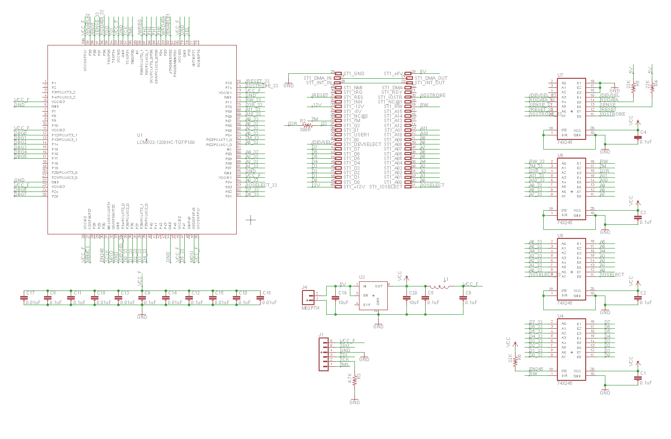
Some hardware background: shown above is a simplified schematic of the card (click for a hi-res version). The FPGA runs at 3.3V, powered from a Micrel MIC5504-3.3YM5-TR LDO regulator. A set of four 74LVC245 chips provide 5V to 3.3V level translation. Three of the chips are configured for unidirectional signals like the address bus and control signals, and the fourth is bidirectional for the 8-bit data bus. Each 74LVC245 has a 0.1 uF ceramic bypass capacitor about 2 mm from its VCC pin. The FPGA has twelve 0.1 uF ceramic bypass capacitors for each of its power/ground pin pairs, and its 3.3V supply is isolated from the rest of the board’s 3.3V supply with a ferrite bead, as recommended in the FPGA datasheet. There are also 10 uF ceramic capacitors on the input and output of the LDO.

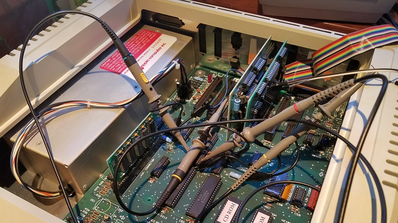
So… where to begin troubleshooting? Based on suggestions from helpful commenters on a previous post, I used a scope to measure the Yellowstone card’s GND and 3.3V relative to a ground point on the Apple IIe motherboard. They both looked pretty noisy, with peak-to-peak oscillation of 680 mV for Yellowstone’s ground and 460 mV for 3.3V, at the moment Yellowstone begins to drive the data bus. But surprisingly I also observed virtually the same oscillation when Yellowstone was *not* driving the data bus and the Apple II was idle – shown in the trace above where where light blue is GND and pink is 3.3V. Then for comparison I examined a standard Disk II controller card, when Yellowstone wasn’t installed in the computer. On the Disk II card, while the Apple II was idle, I measured 600 mV of oscillation on GND and 280 mV on 5.0V. I’m not sure how to explain all this, except to note that Yellowstone’s supply oscillations don’t seem dissimilar to other cards.
At this point I tried a few quick experiments:
- Adding a 47 uF electrolytic capacitor across the Yellowstone card’s 3.3V and GND supplies didn’t make any noticeable difference.
- Connecting an extra ground wire between the Yellowstone card and a ground point on the motherboard helped a lot. The frequency of crashes after reset dropped from 90% to 20%. Hmmm.
To check the data bus voltage levels and timings, I used a 4-channel scope:
- Channel 1 (yellow) – /IOSELECT – Asserted when the Apple II wants the card to drive ROM data onto the bus.
- Channel 2 (light blue) – Phi 1 – 6502 clock signal.
- Channel 3 (pink) – Phi 0 – 6502 clock signal. A read operation terminates at the rising edge of Phi 0.
- Channel 4 (dark blue) – A bit on the data bus, either D0 or D7 depending on the test.
/IOSELECT was measured at the card. Phi 0 and 1 were measured directly on the 6502. The data bus was measured at the motherboard’s 74LS245 buffer, chip UB2 on the Apple IIe motherboard.
To make a long story short, everything looked mostly fine, and I’m stumped as to why Yellowstone crashes when other cards are present. Here’s a selection of scope traces.

As a starting reference, the trace above shows a real Liron card with no other cards installed. When /IOSELECT is asserted, D0 goes high about 64 ns later. It overshoots to 4.7V before settling back to 3.8V. After the rising edge of Phi 0 and /IOSELECT is deasserted, the data bus stays high for 270 ns more. I suspect this is bus capacitance holding the old value while nothing is actively driving the bus, as opposed to the Liron card actually driving the bus beyond when /IOSELECT is deasserted.

Here’s the Liron card driving a logic low voltage on D7. The signal timing is the same as for the logic high on D0. The low voltage is about 80 mV.
I repeated both of these tests with a Liron and a Disk II card both present, and the results looked basically the same.

Here’s the Yellowstone card, with no other cards installed. The signal timing looks the same as with the real Liron card, including the 270 ns “hold period” after /IOSELECT is deasserted. D0 shows a large overshoot to 5.7V before settling back to 3.4V, which is about what I’d expect from a 3.3V card. While that’s a lower voltage than seen from the Liron card, it’s still well above the logic high threshold of 2.0V for the Apple IIe’s 74LS245 buffer.

Yellowstone driving a logic low. There’s some significant undershoot, then the voltage goes to 0V, and timing looks OK.

Now comes the interesting part: the trace above shows the Yellowstone card with a Disk II card also installed. This is the case that doesn’t work, where the computer crashes during power-up. I expected to see something wrong on the scope trace, but I didn’t. It looks very similar to previous test with Yellowstone by itself. The signal timing is the same. The high voltage overshoots to 5.4V before settling back to 3.3V.

Finally, here’s the Yellowstone card with a Disk II card also installed, driving a logic low. The bus voltage goes to 0V. It looks the same as the case when no other cards are installed.
So what now? The only thing that looks maybe concerning in these traces is the large amount of overshoot from Yellowstone when driving a logic high voltage. But the overshoot is actually less severe when a second card is installed, not more severe, which doesn’t fit the pattern of more cards leading to more crashes.
Maybe the bus voltages are only bad at certain moments, when a specific value is driven onto the bus, or some particular combination of control signals occurs? That’s possible, as my test was only able to capture the very first access to card ROM during a boot-up. If there are bad voltages appearing later, I wouldn’t have seen them.
Maybe the problem isn’t bad voltages driven on the data bus by Yellowstone, but bad voltages received by Yellowstone from the data bus and from control signals? If the Yellowstone card’s ground were pulled above the Apple IIe’s ground, it would have the effect of raising the voltage threshold for Yellowstone to receive a logic high, and cause it malfunction if signals were received incorrectly. This might explain why attaching an extra ground wire seemed to help. But from what I’ve seen of the logic signals from the Apple IIe, they’re in the 3.8V and above range, which is significantly higher than the 2.0V threshold of Yellowstone 74LVC245 buffers, even when allowing for a few hundred millivolts of ground differential.
Maybe I’m wrong about this being an electrical problem at all, and despite the circumstantial evidence, it’s actually some kind of logic bug?
Read 37 comments and join the conversation37 Comments so far
Leave a reply. For customer support issues, please use the Customer Support link instead of writing comments.
To rule out the logic bug, can you either run no program on your fpga or run a program that does not interact with the board edge signals? Maybe you can modify your existing program but output the signals to registers instead of pins so it’s (in general) drawing the same amount of power? Is there an usused pin that you can some serial data to and view on the scope and detect what is happening on your board when the computer crashes?
I think the FPGA needs to have the normal ROM code, since that’s where the crash is happening.
I’ve discovered one more clue that may be significant, and it points a finger towards the theory of bad voltages *received* by Yellowstone instead of sent by it. I glossed over this detail before, but the ROM code is actually separated into a 256 byte section in an address range dedicated to the slot, and a 2K byte section in an address range shared by all slots. The crash always occurs in that 2K shared section. And just before the crash, Yellowstone’s internal flag that tracks whether it “owns” the 2K shared section switches from true to false, but I think it should have remained true.
A card gains ownership of the 2K shared section whenever its 256 byte private section is accessed. After that, the only way it loses ownership is when the system /RESET is asserted, or the CPU does a memory access to address $CFFF.
I think that due to voltage ringing, ground float, or some other crazy electrical factor, the FPGA thinks that /RESET was asserted or $CFFF was accessed when it really wasn’t. That causes it to think it no longer owns the 2K shared memory space, and to stop responding to memory reads in that address range. Since the ROM code that’s running is in that range, this causes a crash. At least that’s my theory.
It wouldn\’t be the first time there was a timing race condition that occurred in an FPGA that didn\’t occur when separate logic chips are used. Care to share those sections of the FPGA so we can comment on it?
I don\’t think you have to monitor the reset line yourself. The reset routine takes care of disabling the expansion ROM (see $FA7B on page 356 of the IIe technical reference manual, or disassemble your IIe\’s ROM). I hope this is not actually the problem – spurious reset signals seem pretty bad anyway – but it\’s one thing you don\’t have to do.
On the subject of firmware updates from before, I still think the bitstream for the FPGA should fit into 40K. But if for some reason it doesn\’t, a good way to transfer more data is via the cassette port. The default tape read routine reads data at about 10KB per minute (a custom routine can probably read faster) and you can stream an essentially unlimited amount of data this way.
I noticed something with the yellowstone card, which is not occurring on the other cards..
The yellow stone card is responding the clock and /IOSELECT LOW much faster than the other cards, with the standard Apple cards, the logic on the bus transitions occurring 40ns after the /IOSELECT going low, where as Yellowstone is almost immdiately afterwards..
While this shouldn’t be a problem it is something that yellowstone is doing different..
@Jerry the logic is:
reg expansionRomActive;
wire histrobe = ~_iostrobe & (addr == 12'hFFF);
wire clearActive = histrobe || ~_reset;
always @(posedge fclk or posedge clearActive) begin
    if (clearActive)
        expansionRomActive < = 0;
    else if (_iosel == 0)
        expansionRomActive <= 1;
end
@Fluffysheap you're right about handling reset, it's not really necessary since the reset routine strobes $CFFF. I copied the logic from the Liron card, which does directly use the reset signal. And to be clear, I suspect a spurious reset signal only with reference to the card's totally wrong logic voltage threshold due to ground being pulled up. I have no reason to suspect the actual reset signal is bad.
I'm not going to worry much about the JTAG programming yet. The JED file is 344K. Using the Apple II as the JTAG programmer might be possible, although it raises the question of how to get the JED file from the web onto the Apple II first.
@Ben I see what you mean. I'm not sure if that's significant. Yellowstone begins to respond almost immediately at the /IOSELECT edge, although the voltage doesn't reach the final value until after a delay similar to the Apple Liron card.
Ah. You\’ve got a probable race condition. Wires in verilog are not necessarily wires in the FPGA. The optimizer can flatten the signal any way it wants. So the asynchronous reset can be getting glitched depending on how the address lines decode. So _iostrobe may not actually be gating the decode. To be sure, take a look at the equations that the synthesizer actually generates and see what it\’s doing.
I\’ve not used Lattice parts. In Xilinx, I\’d add the comment below and it would force that signal to be in it\’s own logic cell. In your case, I\’d do something like
wire histrobe_addr = ( addr == 12\’hfff );
// synthesis attribute ASYNC_REG histrobe_addr is “TRUE”;
wire histrobe = (~_iostrobe && histrobe_addr) || ~_reset;
Or, just route the signal out of the FPGA to a pin and back in again.
I should have said \”Route the histrobe_addr signal out of the FPFA to a pin and back in again\”
Based on what you stated, \”The card works fine when it\’s the only card in the system\”, rules out a timing or fpga issue. My guess is there is an impedance mismatch with the 74LVC245A based on the analysis you did with the ringing and overshoot/undershoot, (the noise you are seeing with the scope). The 74LVC245A can only drive 3.3V but appears to get loaded down when you add more cards. You may want to redesign using the 74LVC4245A which keeps the 5V/3.3V voltage domains independent.
@Romdump:
That does not prove it\’s not a fpga problem. Putting another card in the system can skew the address lines farther apart from each other if they\’re all not loaded identically, aggravating the race condition.
@Jerry
I don’t know how the fpga could be causing the nasty signal on the Channel 4 (dark blue) trace. There is ringing and overshoot/undershoot which leads me to believe that some sort of impedance mismatch is happening.
@Romdump:
Yes, the FPGA would not cause that ringing. But it would cause the internal flag to change, like Steve mentions.
Those scope leads look really long to me. That could be a lot of the ringing. When I was doing SI measurements on my PCB, I was using a 2.5GS/S scope with 1GHz bandwidth, and the ground was about 0.3\” long. Things looked a lot better then than when I used the normal 3-4\” scope probe grounds.
If the data bus is ringing when it\’s not being sampled, it\’s not really a problem. It\’s not good, but not necessarily the root issue. Things look pretty stable on the rising edge of PH0, when things need to be stable.
Still, since the CMOS drivers are a lot faster now, putting series resistors of ~ 33 ohms could help clean that up. Yes, that would be an improvement worth doing. If he can fix it without another board spin, even better.
@Jerry I don’t see any potential race condition here, can you explain? The address lines don’t change while /IOSTROBE is asserted, and /RESET never gets asserted during normal operation. But I do think the equation is probably unnecessarily complex, and involving fclk is probably unnecessary and maybe exacerbating a problem caused by power supply fluctuations.
@Romdump Impedance mismatch is an interesting theory. Whenever I hear the word “impedance” I break out in a cold sweat, because it always seems to involve me doing something I don’t understand and experimenting with extra resistors with magic values. Unfortunately I don’t think there’s any way I can test that theory or add series resistors without redesigning and building a new board. Which is maybe what’s required, but I’d like to have some confidence that’s really the issue before going to that effort. For comparison sake, none of the other Apple II cards I examined have any series resistors on the data bus lines. But they all use older 5V 74LS series buffers.
I’m going to take another look at the bypass capacitors on the card. I feel like maybe there’s not enough, or not enough in the right places, so there are large local fluctuations in GND and 3.3V that 1) change the effective logic voltage threshold for signals received from the Apple II 2) change the output voltages sent to the Apple II w.r.t. Apple II ground. That would explain everything I’ve seen, I think.
Another idea: there may be a very brief period of output fighting between the FPGA and the 74LVC245 at the moment it changes direction from reading to writing. That would create a big momentary power glitch of the sort I’ve observed.
I’m definitely not the most knowledgeable oscilloscope operator. The ground leads on the probes are the ones that came with them, and the only ones I have. The Phi 0 and Phi 1 signals have the probe hooked directly to a CPU pin. For /IOSELECT and the data bus, the probe hook is too big to directly attach to a pin. Instead there’s a test hook (stolen from a logic analyzer) on the pin, with a 6-inch female-to-female jumper wire connected to the hook, a 1-inch jumper wire at the other end of the F-to-F, and the oscilloscope probe on the 1-inch jumper. The extra wire may contribute to the signals looking worse than they truly are.
Steve — you know a lot more about this stuff than I do, but I was feeling that maybe more and possibly larger capacitors were needed also. And as I said before, I’d consider upgrading the 3.3V regulator since I’m of the “bigger is better” mindset on that one. That said, I think that some variations on your equations that control the OE input on the ‘245 that controls the D0-D7 and the equations that control the ROM selection are probably worth exploring. From what I’ve read, timing on those two things is often an issue in Apple II cards. Some designs on vintage cards I’ve looked at when working on some of my projects have what appear to be extra gates added to add extra timing. Such as signals that are run into both sides of an AND gate which does nothing but add a tiny delay. I could see how data hitting the bus too early or turning off a ROM prematurely could cause issues.
It looks like I was right that romExpansionActive was getting deasserted when it shouldn’t, leading to the crash. I changed the Verilog equations to remove the dependency on RESET and use a two-sample glitch filter, and now the Apple II can power-up reliably with two cards without crashing.
wire histrobe = ~_iostrobe & (addr == 12'hFFF);

reg [1:0] histrobeHistory;
reg [1:0] ioselHistory;

always @(posedge fclk) begin
	histrobeHistory < = { histrobeHistory[0], histrobe };
	ioselHistory <= { ioselHistory[0], _iosel };
end

always @(posedge fclk) begin
	if (histrobeHistory == 2'b11)
		romExpansionActive <= 0;
	else if (ioselHistory == 2'b00)
		romExpansionActive <= 1;
end
Bad news: it still doesn't reliably work. With Yellowstone plus five other cards in the Apple IIe, I was able to boot from a Unidisk 3.5 connected to the Yellowstone card, and also access a Floppy Emu connected to a Liron card. But when I reversed the drives, and put a Floppy Emu on the Yellowstone card and a Unidisk 3.5 on the Liron card, there were a lot of problems. Most of the time the computer would hang after power up. Control-reset would sometimes get it to boot from the Floppy Emu attached to the Yellowstone card, but usually not. Sometimes it would crash midway through booting Prodos from the Floppy Emu. Sometimes the Floppy Emu would spontaneously reboot, or suddenly complain that the wrong firmware was installed, which is crazy. So there are a lot of issues to iron out.
My guess is that I'm still dealing with some kind of power or termination issues here, and the new Verilog equations merely paper over one manifestation of that with the glitch filter. I'm going to need to get to the root of the problem to make any real progress.
Well, it sounds like you have made some progress to me. Perhaps there were just more than one thing going on and you’ve fixed one of them rather than as you say just papering over the problem. Anyway, you’re learning from this experience, right? And I can say that I’m learning just from reading these threads… so that’s pretty cool. I’m definitely looking forward when you make a breakthrough and this project turns into a real product, because it would be way cool to have something knowing as much of the history of the design as this.
Can you turn down the slew rate of the fpga? You don’t need the 100mhz edges in this application. Then you don’t need to impedance match.
@Steve:
FPGAs use a 4 input lookup table to implement their logic. It\’s not actually an AND gate. Think of it as a lot of little rams. If two inputs change at the nearly the same time, you can see the intermediate output. So if the address goes from 01 to 10, there may be a short amount of time where you\’re reading 11 or 00.
To make the 13 inputs of logic, you\’ve got to stack 7 logic blocks to make that happen. Unless the strobe is at the top level, it may not be gated. And since you were feeding that output to the reset of the flip flop, a really short pulse would reset the flop.
Now that you made histrobe synchronous for two clock cycles, that should avoid the issue.
Yes, the long scope wires will make things look definitely worse. Having the \’245 and the FPGA fighting on 8 data lines would really create a power spike. Fixing that would
Is the fclk signal a clock just for the fpga, or is it related to the apple bus? I didn\’t see a synchronizer flop on _iosel, is there one?
@Vincent the FPGA slew rate is set to “slow”, but I’m not sure it matters here since the FPGA isn’t driving the data bus. It’s driven by the 74LVC245.
@Jerry fclk is the 7 MHz clock from the Apple II. _iosel is synchronized with the ioselHistory buffer, though I’m still not convinced this is necessary, since all the signals come from the same clock domain.
I’ve decided to focus my attention on the big overshoot on the data bus, and the related oscillation in the Yellowstone 3.3V supply. Even though I’m not sure these are causing “the problem”, they’re something I can see and measure, so I can do experiments to test the effect of various changes.
– Changed FPGA keeper mode, logic level, and drive strength: no effect
– Added 47 uF electrolytic capacitor between card’s 3.3V and GND: no effect
– Added two extra ground wires from the card to the Apple II motherboard: no effect (surprising since this helped an earlier test)
– Permanently disabled the ‘245: data bus overshoot disappeared (obviously, since nothing’s driving it) but 680 mV supply oscillation remained.
– Loaded FPGA with a dummy program that does nothing: 400 mV supply oscillation
Some other ideas, before I give up and redesign the whole card:
– Replace the ferrite bead with a straight wire
– Retouch all the solder joints
– Build a second identical card for comparison
– Intentionally delay driving the data bus until a short time after /IOSELECT is asserted
– Wave a dead chicken over the card, pray to the electronics gods, etc.
I don’t know enough about the ferrite bead to make any kind of intentional judgement.
Retouching solder joints couldn’t hurt, but I doubt it will change anything.
Building a second card… Possibly you got a marginal part in there? Who knows.
Adding a delay to /OE after /IOSELECT seems like a good idea
Dead chicken couldn’t hurt.
Something you may want to consider to try before a board redesign. Replace only the one Databus transceiver with the 74LVC8T245. Cut the trace for the B VCC side power supply of 3.3 and use wire wrap wire and solder it to +5v. Also use wire wrap wire and connect the new VCC pin A to 3.3. Other than the additional VCC and GND’s the chip should line up exactly with the 74LVC245A. Just make sure you have enough clearance not to hit the next chip. I know it is a pain to microsolder the TSSOP but you will have your proof to what is causing the bus contention, ringing, overshoot and undershoot. There is a difference between “translating” and “level shifting”. Hope that helps.
Another note. If you really want to clean up the 3.3V supply, put the Oscilloscope in FFT mode and see at what frequency the oscillation is at. Build a LC Low pass filter and filter out the high frequency on the 5V line. Even though you have ferrite bead and capacitor on the output of the LDO, I don’t think it is calculated correctly to remove the high frequency noise from the Apple II SMPS. (You could also probably just replace the ferrite bead with the correct inductor).
Thanks, I’ll look into the possible 74LVC8T245 board surgery. What’s the difference between translating and level-shifting, other than true 5V output on the data bus? Something about slew rates or impedance maybe?
I’m not sure the oscilloscope even has a FFT mode – I’ll have to read the manual. The ring has a period of about 15 ns, but it’s approaching the resolution limit of the scope. The ferrite bead was suggested in the FPGA datasheet, and it’s only on the FPGA’s 3.3V supply. The 74LVC245 chips and other 3.3V components don’t have any ferrite bead or inductor on their supply. There are two separate 3.3V supply regions on the board, sourced from the same LDO, but separated by the ferrite bead.
The ferrite bead might be there to keep FPGA switching noise in rather than external noise out.
The FPGA datasheet lists the raw bitstream at 330 kilobits, which is manageable size for an Apple II. You can do your programming with JTAG, then read out the raw bitstream over SPI and distribute that. The Apple can transmit the SPI data to the Yellowstone over the motherboard \”game\” (really GPIO) port. All you will need is a 4 channel level shifter (txs0104?) and a suitable DIP cable. But you\’ll have to add the shifter and connector in a new board revision. So I mention it now, before it\’s too late!
The JED format is a bulky text oriented format that doesn\’t really give a good idea of how big the bitstream actually is.
With 64K, ProDOS has 43K of RAM available for applications so you might not even need 128k.
Steve,
I don’t think you are convinced on the solution I presented. Let me explain what is is my reasoning and can we prove what I said is correct before we do any drastic things to the PCB.
First off disregard the statement “There is a difference between “translating” and “level shifting””. This doesn’t make any sense and isn’t an explanation. It was 3AM when I wrote it.
Your problem: You are getting intermittent operation as you put more cards on the bus.
You observe on the oscilloscope that probing one of the 74LVC245A databus pin, you are getting a noisy signal. What is the causing this and is the source of the problem?
You observe the 3.3V has noise, (appears to be high frequency), is this the cause?
I said use the 74LVC8T245 and keep separate voltage domains. Why?
Lets first look at the apple II bus. On this bus there is an old school transceiver. This transceiver has a parameter VIH –
(Minimum INPUT Voltage level to be considered a HIGH). I don’t know what is this but you are going to look it up and find out.
The *optimal* maximum voltage the 74LVC245A can send is +3.3V. And I said optimal. As you plug more cards in there is internal leakage reducing this drive voltage.
So what you are going to do is using the oscilloscope is measure the voltage out at the 74LVC245A databus and measure the voltage in at input of old old school
transceiver when it works.
Then add more cards and repeat. Record the results.
What is happening with the voltage? Does it meet the VIH specification of that old school transceiver or is it going below?
As for the 3.3V voltage noise, generally LDO’s are terrible rejecting high frequency noise. If you think this is a problem you have to design a LC Lowpass filter on the power supply rail.
The ferrite bead and the capacitor is a filter but looks like only for the FPGA as you said.
The only reasoning I believe you think the LDO is a problem is that the FPGA is browning out or going into a lockup condition.
Look forward from to your results.
The Apple II bus transceiver is a 74LS245, its Vih is 2.0V. You can see scope traces for the 1-card and 2-card scenarios in the post above. With the Yellowstone card alone, it drives the bus (measured at the 74LS245 inputs) to 3.4V: https://www.bigmessowires.com/wp-content/uploads/2018/02/DS1Z_QucikPrint5.png. With a second card added, it reaches 3.3V: https://www.bigmessowires.com/wp-content/uploads/2018/02/DS1Z_QucikPrint8.png. I haven’t measured it for larger numbers of cards, but will check it next time. But from what I have seen so far, there doesn’t appear to be any problem reaching the Vih threshold.
I think you might need to resort to a test-only version of the FPGA code. Instead of an implementation of a disk controller, you might need to have a simple configuration that just outputs various bit patterns onto the bus. Say every time you read from the card address it sends a new value. Then you can have the cpu in the Apple check those patterns against the same sequence stored in RAM. It can then identify which sort of pattern is causing an error – or if the data comes through clear, then it’s probably not a data bus problem at all. If it’s reproducible you can set up the scope to capture the actual problem signal. And if it crashes the Apple then you know you’re pushing some sort of horrible signal onto the bus.
You can go the other way too: have the Apple send data to the FPGA. It’s just going to be a little less convenient to get the results back out since you don’t have a display plugged into the FPGA…
To rule out the databus I am thinking you should do what @Fluffysheap advise. Write a simple confidence test in the fpga. What ever you write to the fpga is saves that value and when you read it back it gives you that value. Hammer the bus and see what the results.
I don’t want to dissuade you from doing experiments, but I can’t see how an 8T245 level translator can possibly do a better job than the LVC245A. You’ve already verified that the LVC245A is driving the bus high well beyond the required 2.4V (to guarantee 2.0V Vih for receivers). If anything, since an 8T245 would actively drive high to near 5V, any problems with overshoot would likely get worse.
I agree with Fluffyheap’s suggestion to load simpler test code into the FPGA to act as a bus exerciser.
If overshoot is the problem then the 8T245 likely won’t help. I don’t really think high level signals are likely to be the problem at all. The bus is TTL and it’s kind of hard to not supply enough high level voltage because TTL is “naturally” high to begin with. Low drive is much more significant.
The one major difference with the 8T245 is that it for the bus side, it has a 5V supply that would be partially isolated from the 3.3V that everyone is talking about. It shares the same ground, though, so not truly isolated.
The transceiver on the Apple side is an LS series part that will tolerate up to 7V for short periods. I don’t see how you could overdrive this with a 3.3V output no matter what sort of overshoot you have.
I am wondering if the overshoot is caused by the long ground leads on the oscilloscope probe and not the source of the problem. It was speculated before that it was a timing issue, and adding more cards exacerbated the problem. Until Steve gets a basic “bus exerciser” we won’t know where the problem lies. The other speculation is that the LDO is browning out.
It would be interesting if the observed overshoot is a phantom effect of the scope leads. The ground leads are about 4 inches long – is that longer than normal? The other signals I’ve measured with the same probes don’t show such overshoot. Unfortunately I likely won’t have time to experiment with this further until next week.
Steve:
Maybe make a resistive divider ‘probe’. It would be far better at showing you what is happening than those 1x or 10x high Z probes that came with the scope.
– Get about 3m long 50 ohm BNC – BNC cable. RG-174 (about 3mm thick) cable is nice for this purpose, the thicker stuff works but is harder to probe with.
– Cut it in half giving you 2 pieces 1.5m long with a BNC on one end.
– Connect about 50mm of wire to the braid for ground on each one.
– Use an 1/10 watt or 1/8 watt 950ohm (or there abouts, I use a 390 and 570ohm in series, or just a 1k in a pinch) resistor from the centre conductor to 50mm of ‘probe’ wire.
– Tack solder the ground right to the LVC245, and the ‘probe’ wire right to the signal.
– set the scope channel on 50ohm termination.
– The scope will read 1/20th voltage, or 1/40th if you use 2k series resistors instead of 950ohm. 950ohm in series and 50ohm scope termination form a voltage divider, and the 50ohm scope termination completely absorbs the cable reflections, both in theory and in practice (that is parasitics don’t seem to be a problem).
This will load the signal with 1k ohm resistive, but should not cause you any problems… 3.6mA will flow. Your 1x probe was already loading the signal because of it’s rather high capacitance. If 1k does load it, just use 2k ohm series resistors instead. If you use 950ohm 1/10w resistors and keep everything neat, you will easily have useful flatness out to 1GHz or more, and a ‘probe’ capable of showing you edges 1ns rise time. Even with 100mm of ground wire, you will only ring for a few 100ps.
I use this a lot, last week to look at some 125Mbps digital signals… the results are so square you’ll think it must be not showing you the real signal… but it is. The spice deck below shows you what to expect.
The effects of limited bandwidth in the scope work in your favor to make it work -slightly- better than the simulation predicts. If you run the simulation (I use MacSPICE), you’ll notice a ground bounce that isn’t really there in the circuit… this is the sort of thing you might be seeing and the reason to build and try ‘better’ probes. The bounce is caused by the scope input parasitic capacitance (modeled here as Cl at 14pF)… if you take that out, or compensate it away (as my scope seems to) the ground bounce disappears. Comments in spice are lines that start with *
Cheers,
J.
jeff:probe jeff$ cat probe.cir
* A simple resistive divider probe
*
.control
tran 10p 40n 0 10p
plot v(100) v(230,231)*20
.endc
*
Vs 101 0 0V pwl ( 0 0 10ns 0 10.5ns 3.3v 20ns 3.3v 20.5ns 0v )
Rs 101 100 .001r
*
* Probe wire inductance approx 120nH / 100mm
Lp 100 120 60nH
Rp 120 130 950r
Lg 0 131 60nH
Cshunt 131 132 14pF
Rshunt 132 131 50r
*
* Lossless cable approximation, about 1.5m=8.2ns at 60% velocity
Tl 130 131 230 231 Z0=50r Td=8.3ns
*
* Scope termination
Rl 230 231 50r
Cl 230 231 14pF
Rpin 231 0 1Meg
.end
Just a comment to point out that the ‘transmission line’ devices in conventional Spice simulators, such a MacSpice, are single EM-mode idealisations. To model a piece of coax cable accurately you need to use two such devices, one to represent the ground-shield mode and another to represent the shield-core mode. The Spice user guide includes an example that models a transmission-line pulse inverter, e.g.:
https://www.macspice.com/ug/secA.html#A.5
Fortunately, coax cables are easy to module as the two modes are independent. If you want to model a twisted-pair, for example, you need to represent the pure common mode and different modes with Spice devices, and also design a network for each end to couple these eigemodes to the real terminals.