

Das ist kein 6502
I received an email from CPU-builder Dieter Müller, describing his very impressive M02 project to build a custom CPU binary compatible with the 6502, using standard 74LS and similar parts. In short, a project quite similar to my own, except that he’s already done it. Take a look at the photos and hardware description on his site http://freenet-homepage.de/dieter.02/m02.htm. He even got the Commodore 64 kernel and BASIC running on the M02.
Read 1 comment and join the conversation7 Segment LED
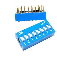
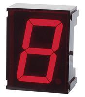
Here’s a job that sounds reasonable enough: connect an 8-wide dip switch to a pair of 7 segment LED displays, so that the 8-bit binary number on the dip switch is displayed as a 2-digit hex number on the LED displays. I didn’t think it would take me too long to configure a GAL to control which segments of the LED displays to turn on, and then wire the whole thing up. Boy, was I wrong.
My basic plan was to connect the dip switch to the GAL’s inputs, and the LED displays to the GAL’s outputs. Easy cheesy.
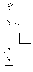
Problem 1. A dip switch doesn’t provide logical 0 or 1 values (0 or +5 volts) that can be connected right to the GAL’s inputs. It’s just 8 switches, each one either open or closed. A simple pull-up resistor circuit is needed to generate a 0 or +5 volt input from the switch position. When the switch is open, no current flows through the resistor, so there’s no voltage drop, and the output terminal is at +5 volts. When the switch is closed, the output terminal is tied directly to ground (0 volts).
One problem with this design is that when the switch is closed, current is constantly flowing from +5 through the resistor to ground. With a 440 Ohm resistor (the largest I had on hand), 11 milliamps (5 / 440) flows through the resistor. With all eight switches closed, that’s 88 mA wasted. My hack-tastic power supply can probably only supply a few hundred milliamps, so that’s a big fraction of the total available supply.
Problem 10. Decoding a 4-bit number is fairly simple: 4 inputs from the dip, the GAL decodes the data, 7 outputs to the LED display. An 8-bit number using the same approach would require 8 inputs and 14 outputs, but the GAL only has 10 outputs. Doh!
My solution is to share the same 7 outputs between two different LED displays, with an 8th and 9th output to enable one or the other display. Only one display can be illuminated at a time, but if you switch between the displays rapidly enough, it looks as if they’re both illuminated. I used a 1 MHz clock oscillator to switch back and forth between the two displays. The 7 data outputs from the GAL are connected to the positive terminal of the 7 LED segments on each display. The 8th data output is connected to the shared negative terminal of the LED segments in the first display, and the 9th data output is connected to the shared negative terminal of the second display.
To illuminate a display, its shared negative terminal is set to 0, and the appropriate data outputs are set to 1, generating a positive voltage across the LED segments. To deactivate a display, its shared negative terminal is set to a high-impedance (disconnected state), so none of the LED segments will light up regardless of what the data outputs are doing. It would also be possible to deactivate a display by setting its shared negative terminal to 1 (+5 volts), but this would put a reverse voltage across the LED segments. That’s best to avoid, since too large of a reverse voltage can damage a diode.
Problem 11. Writing the logic equations for the GAL to decode 8 input bits into 2*7 LED segments proved more difficult than I expected. My first attempt had way too many product terms per output, and was too complex to fit in the GAL. I did some hand optimization, but it was tedious and error-prone. Finally I found a website with an interactive Java applet for making Karnaugh maps, and used it to simplify the equations enough to fit the GAL. The Java app was nearly as tedious as hand optimization, though, and it took me a long time to finish the simplification.
Problem 100. You can’t just connect a chip’s output pin directly to an LED. Since the diode offers nearly zero resistance, it would be like shorting the power supply to ground if the output pin’s value were a logic 1. Instead, a resistor must be put in series with the LED, to limit the current. Larger resistances will limit the current more, but will also diminish the LED’s brightness. I used 220 Ohm resistors in series with each LED segment, which should result in a current of 23 mA (5 / 220). Most LED’s appear designed to hit their advertised brightness level at about 10-20 mA.
Problem 101. There are a lot of wires to connect! OK, this isn’t really a problem, but I was still surprised at how many wires I needed to cut, strip, and push into the protoboard for such a simple project. 8 from the power supply to the 440 Ohm resistors, 8 from the resistors to the dip switch, 8 from the dip switch to the GAL, 7 from the GAL to the 220 Ohm resistors, 14 from those resistors to the two 7 segment displays, plus the 2 shared negative terminal connections, the 1 MHz oscillator, and a handful of other miscellaneous wires. Ugh.
Problem 110. After I’d finished everything and turned on the power, it didn’t come even remotely close to working. LED segments light up in totally random ways. The same dip settings didn’t even always generate the same results. Changing the MSB of the input changed which display was illuminated. Even just touching the circuit with my hand sometimes caused things to change. I was totally confused. At first I thought maybe I was drawing too much power from my power supply, and the voltage levels were getting out of spec, causing erroneous behavior in the GAL. A lot of poking and probing with a multimeter suggested everything was OK in the voltage department. Then I hunted for wiring errors, but found none. I rechecked all my logic equations as well.
After a very long time, I discovered that the GAL had been misprogrammed somehow, and some of the outputs were using the clock input as if it were a data input. I have no idea how that happened– is the chip failing? Is my chip programmer faulty? Sun spots? I reprogrammed the GAL, and things started working much better. It was still broken, but at least now it was broken in a deterministic way, and it sometimes displayed recognizable digits on the LED displays.
Eventually I discovered several errors in my logic equations that I’d overlooked the first ten times. In one place I’d used an AND instead of an OR, and in another I’d omitted an entire term from the equation. It’s amazing how many times I looked at those equations without seeing the mistakes.
After fixing those, the whole thing was almost working, except for:
Problem 111. Strange things happen with long (and not so long) wires involving cross-talk and noise. I never did satisfactorily explain how the MSB of the data input seemed to be acting like a clock input. When I wired the clock input pin straight to ground, the GAL would still often appear to have been clocked (the active LED display would switch) when I changed the MSB. The problem went away when I used a shorter wire to connect the clock pin to ground, so I suspect it was some kind of cross-talk from the neighboring wire. When I later connected the clock pin to the 1 MHz oscillator, it seemed to work fine.
The disconcerting thing is that the clock wire was not especially long (3 inches) nor close to the MSB wire, except that they happened to connect to adjacent pins on the GAL. If it’s truly that easy to accidentally perform false clocking, then I’m going to have a lot of problems building the full machine.
Problem 1000. Everything was finally working, but I wanted to examine the circuit behavior in more detail. Earlier I mentioned the 220 Ohm resistors I put in series with the LEDs, which should have resulted in a 23 mA current through each LED. I measured the current, and it was only about 6 mA. I also measured the voltage at the GAL’s data output pins, and rather than +5 volts, it was only 3.2 volts. This suggests a problem.
I can’t explain why I saw 6 mA of current specifically, but after reading the GAL datasheet more carefully, I decided I was lucky (?) to get even that much. The chip’s maximum output current per pin at a high (logic 1) output voltage is only 3.2 mA. Exceeding that by nearly 2X explains why the output voltage was dragged down from 5 to 3.2 volts. It’s possible that could damage the chip. At the very least, it doesn’t seem like a good design. I’m still curious why I saw 6 mA and not 3.2 or 23, though. Maybe I reached the maximum amount of current that my power supply can deliver, or maybe the diode itself has some current limiting effect?
The math tells me a 1562 Ohm resistor in parallel with the LED would give me the maximum rated current of 3.2 mA per LED segment. Would that be enough current to get sufficient brightness, though?
Although I didn’t measure it, I think I’m running into similar problems with the shared negative terminal of the LEDs, which is also connected to a GAL output pin. The datasheet says the max current per pin at a low (logic 0) output voltage is 16 mA. If I’m sending 6 mA per LED segment through seven segments with a shared negative terminal, then that’s 42 mA (6 * 7), way more than the rated maximum.
Problem 1001. Now I have something that works, but feels iffy. I wouldn’t incorporate it into a finished computer design, due to concerns about greatly exceeding the GAL’s rated maximum output current. The trouble is, I’m not sure how to fix it without introducing more parts between the GAL and the LEDs to provide and regulate current. I’ve seen ready-made LED driver chips, but they’re always binary coded decimal rather than hex. Whatever the ultimate solution, it feels like an awful lot of work just to display a single byte on a pair of LED displays.
To put a positive spin on this experience, I learned more about the kinds of difficulties and pitfalls I’m likely to encounter when I begin to build the machine on the wire wrap board. It’s much better to face them here on the protoboard, where alternative solutions are easy to try, than on the more unforgiving wire wrap board.
Be the first to comment!Universal Programmer
I got a TOP 2007 universal programmer yesterday, for burning EPROMs, GALs, and Flash memory. Whenever I hear the term “universal programmer”, I imagine a nerd-equivalent of the 1992 movie Universal Soldier, starring Jean-Claude Van Damme. Plot: a mild-mannered C++ programmer gets cybernetic implants and goes on a killing spree.

TOP 2007 Pros: It’s pretty cheap (about $100), and it programs GALs, unlike most low-cost programmers.
TOP 2007 Cons: Horrible, horrible software. I’ve seen slipshod, poorly-translated software before, but this really elevates it to an art form. Maybe 25% of the text isn’t translated at all, and is still in Chinese, including some status and error messages. What text is in English is so poorly translated, it’s difficult to tell what it means. “Driver not ready ,if load it now?” Damned if I know. And what’s a “cussor?” Clicking the close box minimizes the window instead. Reading from a chip overwrites the contents of any data file you previously had open for writing. Lots of options and menu items do mysterious unknown functions, or nothing at all. Device recognition doesn’t seem to work– you have to manually select the right device from a list of hundreds, and pray you got it right.
Despite these issues, programming a 128K Flash memory worked fine. I had problems with some Lattice 22V10D GALs, however. That’s especially frustrating, since GAL support is the whole reason I chose the TOP 2007 over other choices. The 22V10 is on the supported device list, and it does almost work, but not quite. What appears to happen is that it successfully programs all the 5000+ fuses needed to implement the logic expressions, but won’t program the last 20 fuses that configure the output pins to be inverting or non-inverting, registered or combinatorial.
Any sane person would have attempted to return the programmer, or junk it and get a better one. Instead I spent an afternoon trying to reverse engineer the software to see if I could fix the problem. By accident, I discovered that I could program 14 of the 20 unprogrammable fuses by adding extra fuse data to the data file, beyond the number of fuses that are actually in the GAL. I also found that 3 more of those 20 seemed to copy the data from elsewhere in the fuse map. But the last 3 fuses appear permanently stuck at 0. The net result is that with some complicated effort, I can completely configure 8 of the 10 GAL outputs. The other two are stuck in registered, inverting mode. I can probably work with that for most purposes. Worst case, those 2 outputs will just be unused.
GAL Counter: The hardware design calls for a stack pointer that’s a 24-bit up/down counter with output enable. The simplest approach would be to use six 4-bit up/down counters, and three 74LS244 drivers, requiring nine chips total. A better solution would use the hard-to-find 74LS569 4-bit up/down counter with integrated output enable, requiring only six chips. Better still would be to use three 22V10 GALs to make 8-bit up/down counters with output enables, requiring just three chips.
It turns out that programming an 8-bit up/down counter into a GAL is quite a challenge. For starters, there are barely enough pins. The 22V10 has 22 data pins, of which at most 10 can be outputs. I was able to barely cram it in by encoding some of the control inputs into a 2-bit function code. But the bigger challenge is that the logic equations for computing the new value of each counter bit require more product terms than the GAL supports. My equation for the MSB of the counter includes 19 AND terms all OR-ed together, but the 22V10 supports at most 16 terms. Here’s my equation:
/q7 := f1*f0*/q7 + /f1*/cet*/q7 + f1*/f0*/d7 + /f1*f0*cet*q0*q1*q2*q3*q4*q5*q6*q7 + /f1*f0*cet*/q7*/q0 + /f1*f0*cet*/q7*/q1 + /f1*f0*cet*/q7*/q2 + /f1*f0*cet*/q7*/q3 + /f1*f0*cet*/q7*/q4 + /f1*f0*cet*/q7*/q5 + /f1*f0*cet*/q7*/q6 + /f1*/f0*cet*q7*/q6*/q5*/q4*/q3*/q2*/q1*/q0 + /f1*/f0*cet*/q7*q0 + /f1*/f0*cet*/q7*q1 + /f1*/f0*cet*/q7*q2 + /f1*/f0*cet*/q7*q3 + /f1*/f0*cet*/q7*q4 + /f1*/f0*cet*/q7*q5 + /f1*/f0*cet*/q7*q6
cet is the count enable (active high). F=00 means count down, F=01 means count up, F=10 means load, and F=11 means no change. So this crazy equation says that bit 7 should be zero if we’re not changing and the current bit 7 is zero, or we’re trying to count up/down but counting is disabled and the current bit 7 is zero, or we’re loading and the input bit 7 is zero, or we’re counting up and the counter is at 11111111, or we’re counting up and the the current bit 7 is zero and any of bits 0-6 are zero, or we’re counting down and the counter is at 10000000, or we’re counting down and the current bit 7 is zero and any of bits 0-6 are one. Phew! If you can simplify that to 16 product terms, you’ll win a prize. Maybe I should create a truth table with 4096 entries, and build a Karnaugh map. Or not.
I need to take another look to make sure there isn’t some clever way I can simplify the equation to get under 16 terms. If not, then I’ll probably either make four 6-bit up/down GAL counters (which would be a little strange, since bytes would be awkwardly divided among different GALs), or six 4-bit up/down GAL counters, essentially replicating a 74LS569 in a GAL. So far I haven’t found any place that has 74LS569s is stock.
Read 5 comments and join the conversationSchematics
I’ve started creating schematics for the machine, using an evaluation version of CSiEDA 5. Making a real schematic that shows all the parts, pins, and interconnections is amazingly time-consuming, but it’s essential if I want to avoid making construction mistakes.
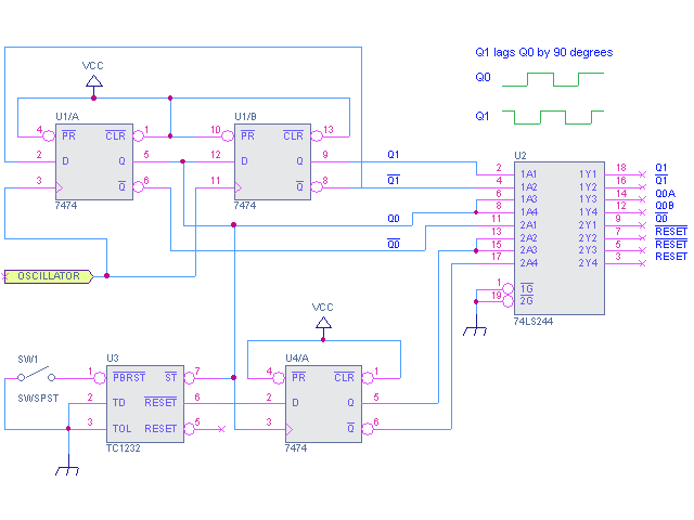
It took me a couple of hours to get familiar with CSiEDA and create this schematic for the clock and reset generation circuitry. A crystal oscillator is used to clock a pair of flip-flops, wired so as to produce two new clock signals, Q0 and Q1, at a quarter the frequency of the oscillator input. Q0 is the primary clock signal, and is used by most other clocked components in the system. Q1 lags Q0 by 90 degrees (one-quarter of a cycle), which is useful for generating other timing signals. The clock signals are buffered by a 74LS244, which has a higher drive current than most TTL chips, meaning each output pin can drive up to 16 other TTL inputs. Some signals appear on multiple ‘244 output pins, where I expect to need them at more than 16 inputs elsewhere in the system.
A Microchip TC1232 supervisor chip is used to generate the /RESET signal. Whenever the +5V input to the TC1232 is too low (during power-on, power-off, or power glitches), it forces the /RESET signal active for about 100ms, restoring the machine to its initial state. It also has an input for a reset switch, with built-in pull-up resistor and debouncing circuitry. The /RESET signal is clocked through another flip-flop, so the rest of the system will only see /RESET change at a clock edge, rather than in the middle of a clock cycle.The TC1232 also has a “watchdog” feature that can be used to auto-reset the machine if it crashes. The CPU is expected to toggle the TC1232’s strobe (/ST) input periodically to indicate that it’s still alive. If too much time passes without /ST being toggled, the TC1232 will force the /RESET signal active. I don’t plan to use this feature, so I’ve tied /ST directly to the clock signal, so it will always be toggling.In the final implementation, the flip-flops and 74LS244 may all be replaced by a single GAL, but the functionality will remain the same.
Read 2 comments and join the conversationFinal Design Tweaks?
I’m trying to finish up the final hardware design now, so I can get started with actually building this thing. Although it will probably never be truly “done”, I don’t want to end up ripping out half the components and wiring to accommodate some new design feature I should have anticipated in the first place.
Here’s what I’ve been considering:
Improved condition code register: I could use a GAL to replace the 4-bit shift register with a custom dual parallel-in, parallel-out register. That would make it possible to load and store the entire CC register in a single clock cycle, instead of shifting data in/out over multiple cycles. The savings would help speed up the BRK and RTI instructions used during interrupt processing, shaving a total of 9 clock cycles off the total time needed to invoke an interrupt service routine and then return to the original program.
Conclusion: Skip it. I expect that a typical interrupt service routine will be tens of instructions long, taking probably 50 to 100 clock cycles, so a savings of 9 clock cycles isn’t that compelling.
Zero-page addressing: The 6502 CPU, from which I’ve borrowed the assembler syntax, has a mode known as zero-page addressing. Instructions using this addressing mode have an implied high-byte of zero for the address, so only the low-byte is specified. This means the instruction requires one less byte, resulting in more compact program code. On the 6502, zero-page addressing instructions also execute in fewer clock cycles than their absolute addressing counterparts. It’s sort of like having an extra 256 registers (the size of the zero page) that can be manipulated with a speed somewhere between true CPU registers and generic memory locations.
To gain a speed benefit from zero-page addressing, the BMOW hardware would require a change to permit zeroing of the high-byte of the address register simultaneously with loading of the low-byte. It would probably also require some tweaking of the memory mapping and reset circuitry, since page zero is currently part of ROM, and the machine begins program execution at memory address 0 after a reset.
If a program could be written such that one in every four instructions employed zero-page addressing, then I estimate it would be about 8% smaller and 6% faster than a program that never used zero-page addressing. In the limiting case where every instruction employed zero-page addressing (not realistic), the program would be 33% smaller and 25% faster.
Conclusion: Skip it, mostly. A typical improvement of under 10% doesn’t seem worth the hassle of changing the hardware design yet again. I may still choose to implement the zero-page addressing mode instructions later as a software-only change (new microcode), which would provide the program size savings, but no speed benefit. It would just substitute a clock cycle where the high-byte of the address register is loaded with some constant value for a cycle where the high-byte would otherwise have been loaded with a byte from the program code.
Add a Y register: I’ve been talking about this for a while, and I think I’ve figured out how to shoehorn a Y register into the left ALU input, where it must be in order to work as intended. The left input already has 4 possible sources, and with no spare control ROM outputs, and I was originally stumped as to how to support a fifth source for the left input.
My solution is to make X and X7 (a pseudo-register containing X’s sign bit) share a single enable signal from the control ROM. This signal would be AND-ed with the load enable signals for PCHI and ARHI, the high-bytes of the program counter and address register, in order to create the individual enable signals for X and X7. If the load destination were PCHI or ARHI, then X7 would be enabled, otherwise X would be enabled. While this is arbitrary and potentially limiting, in practice it mirrors exactly how X7 is already used for address calculations by the microcode. With X and X7 now sharing a control signal, there would be a free one for the Y register.
Conclusion: Do it. While the solution is a bit ugly, it’s relatively isolated. Adding Y will give the machine three general-purpose data registers rather than two, which is a significant improvement that should enable writing substantially faster/simpler programs. It will also make it much easier to port 6502 assembly programs to BMOW.
More than 64K Memory: 64K is the standard memory space for an 8-bit machine, but something larger would open up many interesting possibilities related to multi-tasking, for which 64K is probably too small to be practical. It would also allow the creation of single programs operating on larger data sets. Realistic values for the total amount of memory are in the 128K to 4MB range, assuming the use of standard SRAM.
A key consideration is how the extra memory should be addressed. One option is to have a separate segment register to hold the highest address bits. This register might be explicitly loadable by programs, or might be controlled by the OS, with each process given a separate segment. With this scheme, the bulk of the instructions would still use 16-bit addresses, and the segment register would presumably be altered infrequently. The alternative is to change all the instructions to use 24-bit addresses, providing for a totally generic 4MB address space. That would negatively impact program size and speed, however, due to the extra byte of address data in most instructions. Fortunately these approaches all require the same underlying hardware, with the differences lying entirely in the instruction set design and microcode.
Conclusion: Do it. The extra hardware needed is trivial, and the decision regarding how to use the additional memory can be made later.
But wait, there’s more! On top of these four issues, there are several other half-conceived ideas flying around my head as well:
- Direct connection of a keyboard and monitor (or LCD panel?), instead of using a PC as a terminal.
- Compact flash or IDE-based file storage.
- Integration of a real-time clock with timer interrupts.
- Two-phase clock. Investigate the necessity of buffering for clock signals due to TTL fanout limits.
- Physical construction. I need a case, a power supply, on/off switch, reset button, maybe a fuse? The case must also provide easy access to all the hardware, as well as space/power/mounting points for future add-ons I haven’t yet thought of.
I think I’m getting a little carried away. It’s time to build the basic machine and get it working, then I can return to these other ideas.
Be the first to comment!Protoboardin’
My long-awaited delivery of hardware arrived yesterday, including a protoboard, tools, and about half the components I need to build the machine. I’m using the protoboard to try various test circuits, before I construct the real thing on the wire wrap board. Last night I geeked out with the protoboard, and threw together some sample circuits.

I cut the tip off an old 9V laptop power supply, and wired it to the Vcc and ground terminals of the protoboard. Then I used a 5V voltage regulator and some capacitors (at right in the photo) to get a smooth 5V supply for the other components. The silver rectangle is a 1MHz clock oscillator. The yellow chips are resistors used to limit the current through the LED, and pull up the voltage at the push-switch. The black chip is a 4-bit counter. I wired the push-switch to the counter’s clock input, and the LED to the lowest bit of its output. Every time I press and release the switch, it clocks the counter, the low bit switches between 0 and 1, and the LED toggles off and on. It’s digital baby!
Be the first to comment!