

Multitasking
Buddy Betts had some interesting thoughts about multitasking on BMOW. That’s so far off in the future that it’s probably useless to speculate about it now, but what the heck. Running several programs at once would require:
- A timer interrupt that fires periodically, to initiate task switching.
- Some way to clear the timer interrupt, so exiting the interrupt service routine doesn’t immediately jump back into it.
- An ISR (dare I call it an operating system?) that saves the processor state for one task, and restores the processor state for the next task.
- Some dedicated place to store the processor state of tasks.
- Relocatable code, or segmented memory, or virtual memory, so that the address spaces of programs won’t collide.
Unfortunately, restoring the complete processor state of a task is impossible with the current hardware design. If you look at the block diagram way down at the bottom of the page, you’ll see that there’s no way to load the stack pointer registers with an arbitrary value. That was intentional, because I didn’t need it before, and it meant the machine had exactly 8 possible load destinations, which could be encoded into 3 control ROM bits. Servicing an interrupt involves pushing more data onto the existing stack, then popping it off at the end of the ISR, but never setting the stack pointer to a completely different value. Task switching requires switching between totally different stacks, however. I could make the SP loadable, but then I’d have 10 load destinations (with SPLO and SPHI), requiring 4 control ROM bits (could be a problem), and a larger mux.
I’m beginning to realize that control ROM outputs are precious commodities, since new hardware capabilities tend to require new control inputs, but there’s a hard limit on the number of outputs from the control ROM (8 bits per ROM, and I have 3 ROMs).
A dedicated place for stored processor state isn’t any problem in theory, although it implies an OS-reserved area of memory, and some way of preventing programs from writing to that memory (or just trusting the programs to play nice).
Relocatable code and/or virtual memory seems like the trickiest issue. With a single program machine, the programs can contain absolute memory addresses and jump locations with no problems. But if the OS can potentially load the program anywhere into memory, the programs will need to account for that. One approach might be to have the OS loader modify the program’s code as it was loading it, adjusting any absolute memory references as needed. That could be difficult. Another possibility might be to add a base pointer register, managed by the OS, and to make memory references interpreted relative to the base pointer. That would probably involve extra hardware or extra cycles to adjust each memory reference.
It might be possible to provide a powerful-enough set of relative addressing instructions that programs wouldn’t need to use absolute addressing at all. After all, I am designing the instruction set, so I can do whatever I want. That would be easy enough for relative branches or jumps (although computing the branch destination would be slower than a branch to an absolute address), but I’m not sure how global program variables would be handled. You might still need a base pointer anyway.
A simpler approach might be to use a larger SRAM, and segment memory into a fixed number of blocks, one per process. For example, if I used a 512K SRAM, address lines 0-15 would be the address as the process sees it, and address lines 16-18 would be the 3-bit process ID. The ROM could be configured so that it was mapped into the same location in every processes’ address space. One big drawback of this approach is that each process would get a fixed size address space, regardless of how much memory it actually needed, putting a hard limit on the total number of processes. A more practical drawback is that 5V TTL-compatible SRAMs larger than 128K generally aren’t available, so the machine would be limited to a maximum of 2 or 4 processes, depending on the size of the process address space. Maybe DRAM or other memory technologies could be used instead. I need to investigate how difficult that would be.
Follow up: It seems that André Fachat has already invented a relocatable executable file format (specifically for the 6502) called .o65. See http://www.6502.org/users/andre/o65/fileformat.html for the spec. It embeds extra information in the executable file that enables the OS loader to modify the program’s code as it’s loaded, similar to how I was considering. Given that it was designed for a pre-existing processor, however, inventing a base pointer register or segmented address space out of thin air obviously wasn’t possible, and so a load-time fix-up was the only possible solution.
Be the first to comment!Random Hardware Musings
Here come the GALs: I’ve decided to use GALs in a few places, to make my life easier. GALs (gate array logic) are a simple kind of programmable logic device. Each output pin can be programmed to compute an arbitrary boolean function of the input pins, and can also optionally be clocked like a flip-flop. You could accomplish the same thing with an assortment of individual NAND or NOR gates and flip-flops, but using a GAL really helps reduce the number of required components. A GAL is ideal when you need to compute lots of functions like: /ADRSELECT = /BUSENABLE * CLK2 * /LOAD + /BUSENABLE * /STORE + SOMETHING * /ELSE
Initially I resisted the thought of using GALs, since incorporating programmable logic felt a bit like cheating. Once a few programmable elements are incorporated, why not go all the way and implement the entire machine as a single FPGA? But GALs are far simpler than FPGAs, and have been around since 1978. They seem appropriate for the time period of the machine I intend to build. A few GALs will also help me avoid a proliferation of 7400 Quad-NAND gates and similar chips that I’d need otherwise.
More ALU musings: I’ve decided to keep my 74LS181 ALU, rather than switch to the ‘381 as I’d been contemplating earlier. The ‘181 can do increment, decrement, and left shift of a single operand, which are all too valuable to give up. The ‘381 would have saved me the XOR gates needed to compute the overflow flag, but that seems like a small advantage compared to the loss of those handy ‘181 functions. I can easily use a GAL output to compute the overflow flag.
Interrupts: I’ve nearly finished the interrupt design, and the required hardware changes are minimal. The heart of the change is to use a register with a “clear” input as the opcode register. /LDOP and /IRQ will be fed to an AND gate, and the output will be connected to the register’s /CLR input. In this way, whenever the machine is about to load a new opcode, if the IRQ input is asserted, then it will clear the opcode register instead. Opcode 0 will be a special instruction that saves the processor state on the stack and jumps to the interrupt service routine.
That sounds easy enough, but there are a couple of minor wrinkles. First, there is no 7400-family register with load enable and clear inputs. I could use a pair of 4-bit counters instead, configured so that they never actually count, but that feels a bit ugly. Or I could implement a custom register in a GAL.
The second wrinkle is that I need a way to disable interrupts during the interrupt service routine (or any time really). My current thinking is to add a flip-flop for the interrupt enable bit, /IE. The logic for the opcode register would then be /CLR = /LDOP * /IRQ * /IE. Opcode 0 would need to clear the interrupt enable bit, and the interrupt return opcode would need to set it. Setting and clearing the bit would probably require my last unused control ROM output, unless I can think of a clever way to implement it using the existing bits. Rather than use a separate chip for the flip-flop, I’d probably hide it inside (you guessed it) a GAL.
Read 1 comment and join the conversationFirst Hardware
I bought a used Augat wire wrap board off eBay. It’s a huge 2D array of hollow gold pins, 12″ x 7″. Chips are pushed into the component side of the board, fitting the legs of the chips into the hollow pins. I believe it’s intended to be a force fit, so no soldering. On the wiring side of the board, the pins project out about 3/4″ inch, and wire wrap tools are used to string wires between them.
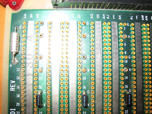
The board has 26 pairs of columns spaced 0.3″ apart (the width of a normal DIP chip), each column 53 pins high. Typical 7400-series chips like the ones I’m using have about 20 pins, 10 on each side. If I packed them in tight, that would give me space for about 5 chips per column pair, or 130 chips total. However, some chips like the SRAM and EPROMs are double-width 0.6″. I also plan to use ZIF sockets for the EPROMs to make it easy to swap them in and out, which will eat up even more board space. Allowing for extra space between the chips and a handful of oversized components, I should still be able to fit at least 60-70 chips on the board, which should be more than enough to accomodate my design.
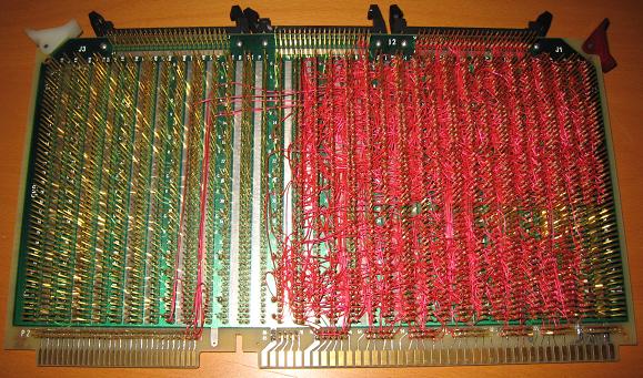
Since this board is used, it has lots of wire wrapping already in place that I’ll need to remove. It also has capacitors soldered between the power and ground pins across half the board. These are marked 0747WC446 in lettering so tiny, it makes me think it’s time to get reading glasses. I’m not sure what capacitance value they are. Maybe it’s best to pull them out? I’m not sure how to find out more about them.
The board also has 3 cable connectors along one side, and a couple of tabs for popping it in/out of a backplane. I’ll probably try to remove these, to get a cleaner look. Although the cable connectors might come in handy some day, if I decide to connect peripheral devices like a disk drive…
Read 2 comments and join the conversationDesign Progress
Programming update: I wrote a simple microcode assembler, and used it to implement a dozen or so common instructions. Then I wrote a few simple programs using those instructions, to count through a loop a fixed number of times, and then branch somewhere else. Woohoo, it’s a computer! I still need to flesh out the microcode assembler a bit more, and get/write a regular program assembler. Since my instruction set is intentionally similar to the 6502, I’m looking at getting an open-source 6502 assembler, and then hacking it as needed for my purposes. Is it enough to assemble all code to an absolute address, or do I need to support the idea of relocatable code, libraries, and linking?
ALU musings:I had planned to use a 74LS181 ALU, and my Verilog model reflects this. I’m now realizing it has a couple of drawbacks. For one, its A=B output is asserted true when the result of the ALU operation is (binary) 11111111, not 00000000 as you would expect from testing equality by computing A-B. I can get around this by testing for equality by computing A-B-1 instead (the chip supports this as a single ALU op), but then I can’t use the result of other non-compare operations to see if they’re zero. For example, a handy pattern would be to sit in a loop, decrementing a counter each time, and branching back to the top of the loop if the counter isn’t zero:
       LDX #04

LOOP: ; do something useful

DEX

CMP #00 ; '181 would require an explicit compare against zero here

BNE LOOP
I need to test for zero (and equality) by testing if the ALU output is 00000000, which I can do with an 8-input NOR gate, and ignore the ‘181’s A=B output. Bing! My chip count just increased by one.
I also realized I need an overflow flag from the ALU, to signal when the result of a signed addition/subtraction is outside the range -128 to +127. The regular carry flag performs a similar job for unsigned arithmetic, but is no help here. An overflow flag can be constructed from XOR-ing some of the input bits with the output and carry, but that would add even more chips to the design.
Enter the 74LS382. It’s very similar to the ‘181, but it jettisons the useless A=B output, and provides an overflow output instead. It also requires just 3 mode select input lines, compared to 5 needed by the ‘181, reducing pin count and required microcode space. It does this by providing fewer functions that it can compute, but it has all the important ones. The only useful functions on the ‘181 not supported by the ‘382 are bitwise negation (1’s complement) and left shifting. You can simulate bitwise negation by XOR-ing with 11111111, so that’s no problem. Left shifting can be accomplished by adding a number to itself, although given my design, that will require an extra clock cycle to copy the number to the temp register first. Given that I was planning to implement right shifting as 7 left shifts, then doubling the cost of left shifts is a problem. But if I can find a work around for right shifts, then I’ll switch my design to use the ‘382.
Interrupts: Bill Buzbee suggested I look at what it would take to support interrupts. I need to find a good source for explaining the theory and practice of interrupts on similar 8-bit computers, because it’s not totally clear to me how they’re intended to be used. My possibly broken understanding is that an external interrupt signal prevents the CPU from loading the next program instruction. Instead, it checks an interrupt vector for the address of an interrupt handler to run. Presumably the vector is stored in RAM rather than ROM, so application programs can install their own interrupt handlers. The interrupt handler would do, um… something about the interrupt. Finally, control would return back to the original program at the point where it left off.
I think this implies that the interrupt handler saves the current state of the registers and condition codes, and restores them when done. This could be a problem, since my design lacks any way to set the condition codes directly. It also implies a way of preventing another interrupt from happening while in the middle of processing the first interrupt. And it implies a way of signaling that the interrupt handler is done.
I guess the whole process could be viewed as a forced subroutine call. It wouldn’t be hard to create a machine instruction that does something similar to JSR, but with indirect addressing, and an implied address. The tricky part would be inserting this instruction into a running program in response to the interrupt signal. Maybe a mux on the input to the OP register, and use the interrupt line to select between the memory data bus and a hardwired IRQ opcode?
Be the first to comment!First Simulation
It simulates! I completed the Verilog description of the machine, and after fixing one place where I’d used an active high instead of an active low enable single, it worked like a champ. I implemented the microcode for NOP, JMP (absolute), and HALT. I was able to run this simple program from ROM: NOP
LOOP: NOP
JMP LOOP
Of course I don’t actually have an assembler or any other software tools, so I couldn’t write the program symbolically like this. My test program is just a bunch of hex numbers entered by hand into a text file. That’s marginally tolerable for a 5-byte assembly program, but writing microcode that way gets old very, very quickly. Each line of microcode is 24 bits wide, and keeping track of what every bit means in my head, for every line of microcode in even a simple instruction like JMP, is near impossible. I need to write a quick-and-dirty microcode assembler before I go any further.
Here’s a simulation trace of the machine booting up and executing the above program.
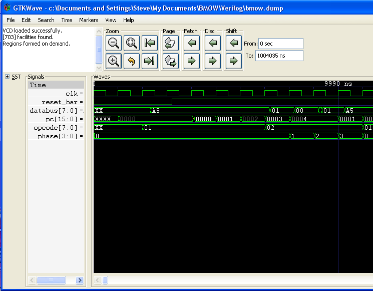
I used the awesome free tools Icarus Verilog for compiling and simultating, and GTK Wave for analyzing the waveform results. I put basic timing information into the hardware model as I was constructing it, using Verilog delays to make outputs lag inputs by the worst-case propagation delay cited in the datasheet. Theoretically, I should be able to use this to determine a lower-bound on the machine’s clock speed: just crank up the simulated clock speed until it stops working.
While completing the Verilog description of the machine, I found that I needed more “glue logic” chips for computing simple boolean functions than I’d like. Decoding memory addresses to enable the appropriate memory-mapped hardware required three different chips, and I needed several more to help with hardware initialization signals during reset. I ended up needing at least one each of NAND, NOR, AND, and OR. If I were more clever, I think there’s a lot of opportunity to clean up this logic and reduce the required chip count. Maybe I should look at using a PAL (or PLA? are they the same thing?) to compute all my simple boolean functions on a single chip, although it might be a lot slower.
I had an idea for a way to add a Y register to the machine, with just two more chips: a ‘377 register and a ‘244 driver. The obvious place to add it as at the right ALU bus, where there are presently only 3 inputs, but the control ROM encoding allows for 4. The problem is that the control ROM only allows for 8 “load destinations”: A, X, T, PCLO, PCHI, ARLO, ARHI, MEM. My idea was that I could have ARLO chain-load from ARHI instead of from the data bus, with just a single load enable signal instead of separate lo/hi enables. That would free up space for a Y load enable. Of course it would mean the machine could never load ARLO and ARHI independently: it would always have to load them one after another, first ARLO, then ARHI. I’m not sure if that’s practical, and I suspect it may not be, at least not without a performance penalty.
Construction update: I’ve started looking further into how to assemble this thing. I’m planning to use wire-wrap construction, even though I have no experience with it, since it seems like that’s what everyone else does. I found some used wire wrap tools and boards on eBay, and I’ll try to pick up something cheap. I’m not sure yet what I’ll mount the board inside. Maybe an old PC case, or a vanilla plastic project case, or a wooden box. It needs to be something to which I can mount some LED displays, switches, and buttons, with a little bit of homebrew bling, even if it doesn’t look like the bridge of the Enterprise.
Read 1 comment and join the conversation6502 Inspiration
The design of my machine has been significantly influenced by the 6502, the microprocessor used in most 80’s home computers, and the one with which I’m most familiar. There are no published descriptions of the 6502 internals that I know of, however. The documentation describes the instruction set interface, not how those instructions are implemented.Still, I was able to infer a lot from the nature of the 6502 instruction set and addressing modes, and the known clock cycle requirements for the various instructions. I plan to have an instruction set very similar to the 6502’s, to make it as easy as possible to port code. That may seem uncreative or like cheating to some, but I don’t see a good reason for inventing my own oddball instruction names, conventions, and assembler syntax just for the sake of being different. So where possible, I’ll make instructions that look and act like their 6502 counterparts.
I also plan to support at least these addressing modes:
| Mode | Example | Description |
| implied | INX | operand implied |
| absolute | LDA $HHLL | operand is address $HHLL |
| absolute, X-indexed | LDA $HHLL,X | operand is address incremented by X with carry |
| immediate | LDA #$BB | operand is byte (BB) |
| indirect | LDA ($HHLL) | operand is effective address; effective address is value of address |
| PC-relative | BEQ $BB | branch target is PC + offset (BB), bit 7 signifies negative offset |
| stack-relative, X-indexed | LDA SP,X | operand address is stack base incremented by X with carry |
All but stack-relative addressing mode are from the 6502.
Despite the similarities in instruction set and addressing modes, my machine will be inferior to the 6502 in that it lacks a Y register, zero-page addressing, decimal mode, interrupts, and the capability to set the stack pointer and push the condition code flags on the stack, among others. On the other hand, it will be superior to the 6502 in that it provides a full 16-bit stack pointer (the 6502 has an 8-bit SP) and stack-relative addressing mode, which I see as a necessity for implementing programs in languages like C.
I’ve worked out the microcode and timing for a handful of sample instructions, using my proposed microarchitecture design. Here’s how I stack up against the 6502. Where two numbers are shown, the larger number is for the case where a page boundary (256 bytes) is crossed while doing address arithmetic.
| Instruction | Description | 6502 clock cycles | My clock cycles |
| ADC | add with carry, immediate | 2 | 2 |
| JMP | jump to absolute address | 3 | 4 |
| BMI | branch if minus | 3/4 | 4/5 |
| INC | increment memory, absolute, X-indexed | 7 | 7/8 |
| PHA | push accumulator onto stack | 3 | 2 |
| JSR | jump to subroutine, absolute | 6 | 8 |
| RTS | return from subroutine | 6 | 6 |
| LSR | logical shift right 1 bit, implied | 2 | 9 |
| LDA | load accumulator, stack-relative, X-indexed | N/A | 4 |