

Yellowstone Glitch, Part 5: Fix Signal Integrity With This One Weird Trick
All the clues surrounding Yellowstone’s glitching problems seem to point towards a power supply problem with the ‘245 bus driver and/or the SRAM. The good news is that I now have a “solution” that seems to fix the glitches, and gets the board functioning normally. The bad news is that I don’t understand why the solution works, or what the underlying problem is, so I can’t be confident that it’s really gone.
In part 4 I described how the glitch occurs occasionally if the value $FF is read from RAM. Something goes wrong when driving all 1 bits from RAM onto the data bus. So my solution is to handle RAM reads like this:
- Make the FPGA output the value $AA / 10101010
- After 70 ns, enable the ‘245 bus driver to put that value on the Apple II bus
- After another 70 ns, turn off the FPGA output and enable the RAM to get the real value
- At the end of the bus cycle, disable the ‘245 and the SRAM
And it works! I no longer see glitching on the logic analyzer, and Yellowstone now seems to work normally for booting disks on the Apple IIgs. But why does this trick help?
One possibility is a residual 5V on the data bus from the previous bus cycle’s value. When the 74LVC245 turns on its outputs and tries to drive 3.3V onto the bus, but finds that the bus capacitance is already charged to 5V, this will briefly create a condition that violates the maximum output voltage rating of the chip. Maybe it causes unexpected behavior or chip damage. If that’s what’s happening, then pre-driving 00000000 before the real RAM value instead of 10101010 should be best, because it will avoid the condition where the chip tries to drive 3.3V into a 5V bus capacitance. But I tried this, and it actually made the glitching worse than it was originally. Hmm. That would seem to rule out this explanation.
A second possibility is that there’s no violation of any maximum ratings, but that driving 11111111 onto the data bus simply demands a large amount of instantaneous current, which the bypass capacitor and the voltage regulator are unable to handle. So the local 3.3V voltage sinks down and/or local GND voltage gets pulled up, and some chips glitch. The ‘245 and the RAM are the furthest chips away from the voltage regulator on the PCB, so this would make sense. Pre-driving 10101010 before the actual RAM value helps smooth out the supply current spike by preventing all the outputs from changing to 1 at the same time. Any other pattern with four 1 bits should serve the same purpose.
If this is indeed what’s happening, then the real solution ought to be ensuring the ‘245 and the RAM both have really good 3.3V and GND connections back to the voltage regulator and to the board’s bulk capacitor, and also adding some larger value bypass capacitors directly next to each chip. So I did some surgery on the board, adding a 10 uF SMD ceramic bypass capacitor next to the existing 0.1 uF for the ‘245, and running 3.3V and ground wires directly back to the regulator, but it didn’t fix the glitching. That was a surprise, and it would seem to rule out this explanation too.
Now I’ve apparently eliminated both of the plausible explanations for the glitching behavior, leaving me with nothing. Either my testing is flawed, or something else is happening here that’s different from either of these explanations. It’s all driving me slowly insane. Although I now have a work-around solution in pre-driving 10101010, I don’t want to move on until I can explain all this behavior and have some confidence that the problem won’t return.
Read 7 comments and join the conversationYellowstone Glitch, Part 4: The Plot Thickens
I’ve discovered something very useful about the signal glitching problem with Yellowstone: I can reproduce the problem (or a form of it) without booting a disk, and even without any disk drive attached. After many hours, I think I’ve narrowed it down to this:
If the CPU reads the value $FF from any location in Yellowstone’s RAM, it might cause a glitch on many different signals simultaneously.
Reading $FF from Yellowstone’s ROM doesn’t cause any trouble. Reading other values with seven 1-bits from Yellowstone’s RAM may cause a glitch, but it’s less likely than when reading $FF. Reading values with six or fewer 1-bits from RAM doesn’t seem to be a problem.
I wrote a tiny program to store $FF in RAM and repeatedly read it back in a loop, and then examined a variety of board signals while the program was running. There were nasty glitches everywhere. But when I zoomed out the time scale, I noticed that the glitches appeared in regular clusters. And zooming out still further, I made this discovery about the behavior when continuously reading from Yellowstone RAM:
Glitches appear in a roughly regular pattern with a 16.5 ms period. Within that pattern is a second pattern with a 62 us period.
Yup, it’s a 60 Hz pattern with a 16 KHz pattern overlaid. Smells like NTSC video! But I don’t think it’s literally video interference, as I’ll explain in a moment. My guess is it’s an issue with data bus traffic related to the Apple IIgs video refresh.
One more important detail:
Glitches appear almost immediately after the ‘245 is enabled to drive the data bus, and can continue for a long time (hundreds of nanoseconds).
Speculation and Guesses
I’m pretty confident about everything up to this point. The rest is an educated guess:
When the ‘245 is enabled to drive a $FF value onto the data bus, it somehow causes signal integrity problems elsewhere. This might be due to undiagnosed bus fighting, but my hunch is that it’s actually due to the capacitance of the Apple II data bus. From what I’ve read in a few reference books, the bus has a pretty high capacitance, and this is a “feature” that holds the last value on the bus even after nothing is driving it anymore.
If the last value on the bus was 00000000, and the ‘245 tries to drive 11111111, there will be a brief rush of current while the bus capacitance is charged up. But the bypass capacitor on the ‘245 should handle this, I think. Adding more / different capacitors to the ‘245 on my board didn’t seem to help.
I suspect the real problem might be exceeding the maximum ratings of the 74LVC245. It’s a 3.3V chip with 5V tolerant inputs, but the output voltage is only safe to VCC + 0.5V. If the chip turns on its outputs to drive 3.3V onto the data bus, but sees there’s already 5V there, the absolute maximum rating will be exceeded. Maybe this results in 5V feedback back into the 3.3V power supply? Which results in horrible glitching everywhere else?
The Apple II video circuitry uses the data bus to read video memory, in between each 6502 or 65816 CPU cycle. That means the last value on the bus will be determined by whatever the video circuitry just read. This would explain why the glitching appears to follow a pattern with a frequency that matches NTSC video.
Holes in the Theory
This sounds sort of plausible. But when I measured the 3.3V supply with an oscilloscope, the few swings I saw didn’t seem large enough to cause problems like what I’m seeing. Maybe I need to look harder.
This theory also wouldn’t explain why glitches sometimes continue for hundreds of nanoseconds. Surely the parasitic bus capacitance should be fully charged or discharged in less time than that? Maybe it induces some kind of unwanted oscillation in the voltage regulator or other components?
The biggest flaw with this theory is that it doesn’t explain why the glitches only happen when reading from RAM, not ROM. The RAM and the FPGA (which contains the ROM) are connected in parallel to the ‘245. From the viewpoint of the ‘245, outputting a $FF byte from RAM is identical to an $FF byte from ROM.
RAM Supply Current Spikes
The SRAM datasheet reveals that the chip’s supply current is 85 mA when /CS is asserted, but as low as 2 mA when /CS isn’t asserted. My design is constantly switching /CS on and off for RAM accesses, so that’s going to create a very spiky current demand.
As before, I think the bypass capacitor on the SRAM should handle the spiky current, and adding more capacitance there didn’t seem to help my prototype board. So this doesn’t quite fit, but it’s the only reason I can think of why RAM access would behave differently from ROM access.
Confirming and Maybe Fixing
Putting everything together, the theory looks like this: when the ‘245 drives 11111111 onto the data bus, it creates a whole lot of power supply noise, possibly due to exceeding the output voltage maximum rating. Normally this noise isn’t enough to cause problems, but if the SRAM /CS is asserted a short time earlier, it will also create a supply current spike when that 85 mA load is switched on. The combination of these two effects is what pushes the Yellowstone board over the line into glitching territory. And the glitches continue for a couple of hundred nanoseconds, because of… reasons I don’t know.
When I write everything out, this theory actually sounds pretty shaky. But it’s the best I have right now.
What evidence would help prove or disprove this theory? Better measurements of the 3.3V supply? Bus voltages? Current into and out of the ‘245? Some of that would be difficult to measure.
Assuming this theory is right, how might I fix it? It seems like the exact type of problem that bypass capacitors should help solve, but so far I’ve seen no improvement when adding extra bypass caps. Maybe I need to try harder, with different capacitor values and in different locations on the board.
Another fix might be to replace the 74LVC245 with a 74LVT245. It’s basically the same chip, but with a higher current drive and with outputs that are safe up to 7 volts. If I’m causing problems by exceeding the max output voltage of the 74LVC245, swapping for the LVT should resolve it.
Other options might be to use a dual-supply 74LVC8T245, or to add series termination resistors, but both of those ideas would require designing and building a new board revision. Without more confidence that it would actually fix the problem, I’m reluctant to do that yet.
Read 15 comments and join the conversationYellowstone Glitch, Part 3: Train Wreck
This Yellowstone glitching problem has gone from puzzling to frustrating to potentially project-ending. I’m still not exactly sure what’s going wrong, let alone how to fix it, and I’ve nearly exhausted all my troubleshooting ideas. In the hopes that maybe the problem could be explained by damaged hardware, I assembled an entirely new Yellowstone card from spare parts, but it fails in exactly the same way as the original card. Grrrr.
Let’s review the facts here. In limited testing, Yellowstone appears to work great on the Apple IIe for controlling any type of disk drive: Smartport drives like the Unidisk 3.5 or Floppy Emu’s hard disk mode, dumb 3.5 inch drives like the Apple 3.5 Drive, and 5.25 inch drives. On the Apple IIgs it works for Smartport drives and 5.25 inch drives, but dumb 3.5 inch drives almost always result in a crash while booting the disk.
The immediate cause of the crash looks like this: While the computer is executing code from the Yellowstone’s onboard ROM in address range $C800-$CFFF (which is actually internal FPGA memory), the card suddenly thinks it’s been deactivated and that it’s no longer in control of that address range. So it stops outputting bytes, the CPU reads and executes random garbage bytes, and there’s a crash. Yellowstone thinks it was deactivated because it thinks the CPU put the address $CFFF on the bus, which deactivates all peripheral cards. But that’s not true.
For unknown reasons, this problem only ever occurs during a clock cycle when the CPU is reading from Yellowstone’s SRAM chip, although I don’t have any idea why that’s relevant. Nor can I explain why it only happens for 3.5 inch disk drives, and only on the Apple IIgs.
At first I thought it was a clock glitch on Q3 causing Yellowstone to incorrectly see and react to a phantom $CFFF address, and I captured some Q3 glitches with the logic analyzer. But then I started noticing other glitches on other signals, some of which appear tens of nanoseconds before the Q3 glitch. So it’s more likely that the Q3 glitch is a symptom of some other problem, rather than the root cause.
My best guess (but only a guess) is there’s a problem with the 3.3V power supply, and some transient noise on the supply is inducing glitching in multiple locations. With an oscilloscope, I observed a few instances where the 3.3V supply very briefly swung as high as 3.84V and as low as 2.76V, at the same time the data bus driver was enabled. But I’m a bit suspicious of those numbers. My oscilloscope always seems to show wild ringing on signals, no matter what project I’m working on, so I’m thinking that’s at least partly the result of my probes or the way I’m taking the measurements. I made several changes to the bus driver, including advancing and delaying the enable timing, and adding more bypass capacitors with various values, but nothing seemed to make a difference in preventing the glitches.
Without being able to clearly characterize exactly where and when the problem is occurring, my hopes for fixing it are low. I still don’t know whether what I’ve observed on the logic analyzer is the cause, or only a symptom.
The bad news is that I’m running out of ideas about what else to try. This train is headed down the wrong track, and the next stops are Frustrationville, Dead-End Town, and Abandon City.
Read 15 comments and join the conversationClock Glitch, Part 2
I’m still chasing the cause of a rare Q3 clock glitch on the Yellowstone board. I’ve collected some more data that may help point to the underlying cause. It’s quite a puzzle, but I like a good mystery.
I began with some armchair reasoning. A glitch happens when some signal changes state and accidentally causes another signal to change state too, usually due a defect in the board’s design. Glitches don’t appear when all the signals have a constant value. My earlier observations showed that the Q3 glitch always occurred during a read from Yellowstone’s SRAM chip, about 50 to 150 ns after the falling edge of Q3. So what other signals would be expected to change state 50 to 150 ns after the falling edge of Q3? Those would seem to be the only possibly culprits.
I reviewed the Yellowstone design, and the list of signals that could change state during that time window is pretty short. First among them is 7M: a 7 MHz clock that’s provided by the Apple II. I examined what 7M was doing at the time of the glitches, but there was no particular phase relationship I could find between 7M and the Q3 glitch, after reviewing many example glitches. So I think 7M can be crossed off the list. Next is Phi1, another Apple II clock. But reviewing the trace showed that Phi1 never changes during the time period of interest.
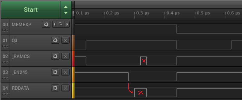
That only left a couple of asynchronous signals as possibilities, including RDDATA, the incoming bit stream from the disk. RDDATA could change state at essentially any time. When I captured a trace including the glitch and RDDATA, I found something very interesting:

I call this the multi-glitch. You can see there’s a glitch on RDDATA before the falling edge of Q3, with a simultaneous glitch on RAMCS, and the glitch on Q3 happening about 140 ns after that. This tells a different story than my earlier data, because it shows that the problem started before the falling edge of Q3. It means the Q3 glitch is just a manifestation of something that went wrong a moment earlier.
At first I thought there was a simple explanation for this: something bad on RDDATA causing cascading problems elsewhere. But although a glitch on RDDATA would cause disk data to get corrupted, it shouldn’t have any effect on RAMCS or Q3. Instead I think all three signals must be getting impacted by sudden fluctuations in the power supply. At least that’s the only explanation I can think of for three signals to glitch at the same time, when they’re logically unrelated and physically separated on the PCB.
The glitching on RDDATA and RAMCS looked unrelated to the actual data on RDDATA, but it always happened about 160 ns after the rising edge of Q3. Applying the same armchair reasoning as before, I wondered what other signals might be changing state when the glitch occurred, and this time I had a better answer. That’s about 20 ns to 80 ns after the board’s 74LVC245 bus driver is enabled, pushing Yellowstone’s output byte onto the Apple II data bus:
Now I think we may finally be getting close to an answer. It would make a lot of sense to see sudden fluctuations in the power supply shortly after the 74LVC245 is enabled. If there’s bus contention, that’s the moment when it’s going to appear. And even if there’s not bus contention, if the bus driver’s outputs simultaneously all change from 0 to 1 or vice-versa, it can create a big current spike. This is exactly why bypass capacitors are important, to smooth out power supply noise from this type of event.
Bus contention on this ‘245 was exactly what caused the downfall of my original Yellowstone effort back in 2017-2018. It was more than two years before I came back to it, identified the bus contention, and fixed it. Or did I? Maybe it’s not completely fixed? So I tried making some changes to advance or delay the timing of the ‘245 enable signal, but it didn’t seem to have any effect on the glitching. Hmm.
Maybe there’s no bus contention, but it’s still a problem when all the bus driver’s outputs change at once. I’m not sure why that problem would only happen when the SRAM chip is being read, but maybe the SRAM also places a sudden load on the supply rail, and the combination of the two effects is too much. Do I have insufficient bypass capacitance on my ‘245 bus driver chip? It’s a 0.1 uF ceramic capacitor, connected by short traces to the chip’s power and ground pins. I could try soldering in some additional capacitors, or capacitors of a different type.
Whether it’s bus contention or something else causing power supply fluctuations, I ought to be able to see the fluctuations on the 3.3V supply at the moment of the glitch. But when I looked, I didn’t see anything. That could be because I used the analog mode of my logic analyzer, which has a very limited bandwidth, rather than a true oscilloscope. I need to keep looking. I feel like I’m getting closer to solving this puzzle, but still not quite there.
There’s still one other possible explanation here: a damaged chip resulting from my earlier fiasco when D5 was accidentally shorted to the 3.3V supply. That could have damaged the ‘245, the SRAM, or the FPGA. They all seem to be working OK now, but maybe there’s some hidden damage, and under the right conditions the ‘245 will go crazy and draw way too much current.
Read 1 comment and join the conversationClock Glitch
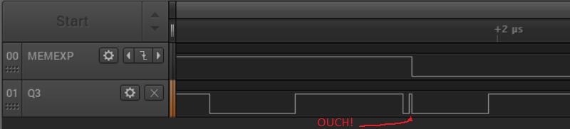
I’ve found a rare clock glitch in the Yellowstone hardware, but I’m not sure how to fix it. This seems to be the source of the “mysterious signal glitching” I mentioned in my previous post, that disappeared after some minor changes to the FPGA logic. From what I can tell it no longer affects the Apple IIe, but pops up rarely on the Apple IIgs, wreaking havoc. I’d suspected a glitch for a while, but I never directly observed it happening until increasing the logic analyzer’s sampling rate to 125 MHz and lowering the logic threshold from 3.3V levels to 1.8V levels. The evidence is shown above.
MEMEXP is an internal FPGA signal that should remain high. Q3 is a 2 MHz clock provided by the Apple IIgs. There’s an 8 ns wide glitch pulse shortly after the falling edge of Q3, and this causes MEMEXP to go low when it shouldn’t. In all my tests, the glitch pulse always occurs during the low period of Q3, between 50 to 150 ns after the falling edge.
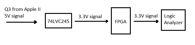
An important detail: The Q3 shown in this logic analyzer trace isn’t actually the FPGA’s Q3 input, because that’s on a PCB trace without any good place to attach a probe. The trace shows an FPGA output that’s been configured to simply propagate the Q3 input. That should be nearly the same thing, but not exactly identical. To complicate matters further, there’s also some level conversion happening. The Q3 supplied from the Apple IIgs is a 5V signal, and it passes through a 74LVC245 to create a 3.3V signal that’s connected to the FPGA. Behold my awesome diagram:
The previous Yellowstone prototype had a 390 ohm inline resistor between the Apple II’s Q3 signal and the 74LVC245. This is something I copied from the design of Apple’s Liron disk controller, although I don’t understand why it was there. None of the other disk controllers that I examined have a resistor on Q3, and I couldn’t find any documentation about a need for one, so I eliminated the resistor in this second generation prototype. Maybe that was a mistake, and is the reason why I’m seeing clock glitching now.
My hunch is there’s a different explanation. I suspect the glitching is caused by other problems on the board, rather than Q3 itself. Maybe there’s capacitive coupling between Q3 and another nearby signal trace. Or maybe my power and ground supplies are bouncing around whenever there’s a big spike in current, like when a bunch of chip outputs switch simultaneously from low to high, and that creates EM noise everywhere. Or maybe there’s some brief contention on the data bus that creates spikes and noise.
I tried playing around with the the FPGA input buffer settings for Q3, in an attempt to make the problem go away. I tried pull modes of KEEPER, DOWN, and NONE, and hysteresis settings of SMALL and LARGE. Nothing helped.
I’m not sure where to go next. I could try assembling a second board, to see if it’s just an assembly problem with this particular board rather than a general design issue. I could look for a way to get a logic analyzer probe directly on the actual Q3 input, which might require fancy soldering, and might also change the behavior. Or a probe on the 5V version of Q3, directly from the Apple II. I could try to patch a 390 ohm resistor onto the board, but it wouldn’t be clean and might create more clock problems than it solves. Or sprinkle some more capacitors around the board, or other analog magic.
Read 4 comments and join the conversationYellowstone Testing With Real Drives
I’m still testing the latest prototype of Yellowstone, my FPGA-based universal disk controller for Apple II computers. After a great deal of poking and prodding, the disk controller is now mostly working with all of the Floppy Emu’s disk emulation modes and with a variety of real Apple II drives. Hooray! But there’s still so much more work to do.
This is version 2.0 of Yellowstone, and it hasn’t exactly been a smooth experience getting it working. First I discovered a layout blunder, where I ran a signal trace right through a power via. After patching that with a razor and some wire, I struggled with mysterious signal glitching in a different section of the board. Some minor changes to the FPGA design made the glitching disappear, but I’m not convinced it won’t return later. Then I discovered a design flaw which means certain types of drives will create a short circuit when plugged into the card’s second drive connector. I’ll fix that in the next revision. Eventually I got the Yellowstone card working with a Floppy Emu, but real drives wouldn’t cooperate. That ultimately proved to be an issue with the width of the read pulses from the drives – they were too narrow to detect reliably. I adjusted the FPGA design to compensate, and now I’m finally in business.
Current status: I’ve had success with an Apple IIe plus Yellowstone booting from a Unidisk 3.5, an Apple 3.5 drive, an Apple Disk 5.25, and a Floppy Emu in its 3.5, 5.25, Unidisk 3.5, and Smartport hard disk emulation modes. The Disk II and Duo Disk should also work, though I haven’t yet tried them. But this is just the very beginning of testing, with a single Yellowstone card in slot 6 and a single disk drive. I haven’t tried writing to the disk, or formatting a disk, or daisy-chaining drives, or using the second drive connector, or anything in the Apple IIGS.
I tried connecting a Macintosh floppy drive pulled from a Quadra 605, and the Apple IIe wouldn’t even turn on. I think I shorted the power supply somehow. This was supposed to work. I’ll look at it more closely later.
Something is still funky with the Apple 3.5 Drive support. Two of the 3.5 inch floppies I tried will boot reliably, but one won’t. But the same three floppies work fine in the Unidisk 3.5. I haven’t yet tried to troubleshoot this one.
It also appears that the behavior changes depending on whether my JTAG programmer is connected to the card, and sometimes it doesn’t work if the programmer is connected. That’s concerning. In the past, I saw something similar with earlier prototypes. I’m not sure if the programmer is holding the FPGA in a reset state, or if it’s an analog problem with the card that’s affected by the presence of the programmer. Another mystery to investigate.
The Apple 3.5 drive and Apple 5.25 drive both sound noticeably different when used with Yellowstone as compared to an Apple standard disk controller. While I haven’t yet determined why, I think this is benign and is due to differences in exactly when and how the disk controller moves the drive head. But when you’re accustomed to disk drives having a certain characteristic sound during I/O, it’s a little disconcerting. The Apple 3.5 drive sounds frenetic, and the 5.25 drive’s familiar buzz-buzz-buzz startup noise is completely different. This latter one bothers me enough that I may try to change it, even if it’s not causing any problems.
Ruminations
It’s hard to believe, but the Yellowstone project will celebrate its fourth birthday this summer. I have to admit I’ve taken on a bigger challenge than was probably wise, and I’m struggling. For me, this stuff is hard – much harder than the Floppy Emu’s development. It’s difficult to maintain motivation when I keep running into one major problem after another, with the goal of “finished” always far away. And the domain of possible problems is huge. One day I’m troubleshooting some software incompatibility with GS/OS, the next day I need to become an expert in FPGA in-system programming, and the day after I’m chasing signal integrity problems in the analog domain. It’s tiring.
There’s still lots to do. All the problems I mentioned above must be examined and fixed. Then there’s a whopping huge amount of testing needed, with a dizzying number of permutations of computers, cards, slots, drives, daisy chain configurations, boot priorities, and software disks. That’s practically guaranteed to turn up more thorny problems that will be difficult to solve. And then I still need to build solutions for in-system reprogramming of the FPGA by end users, and for fast and thorough automated testing during manufacturing. I have some plans for how to handle those, but haven’t yet started any work.
I’m hopeful that while the Yellowstone project isn’t yet “almost done”, it’s at least close to the point where the finish line is visible. I really want to wrap this up and get it out the door.
Read 3 comments and join the conversation