

Tiny CPU in a CPLD
Tiny CPU is a custom “small CPU” design intended for implementation in a CPLD. Such soft CPU cores typically target an FPGA or large CPLD, but the target device for Tiny CPU is a small Altera CPLD with limited logic resources. This constrains the CPU to a minimal set of features in order to fit. It is an 8-bit CPU with only two registers, and a 10-bit address space. The instruction set is a subset of the 6502 instruction set, with modifications to reflect the smaller address space and number of registers.
Download the Tiny CPU file archive, including the assembler and Verilog source files.
Design
The project is split into two halves, originally imagined as separate chips, but now combined into one. The core CPU module is called Tiny CPU, while a companion module called Tiny Device implements address decoding, bank switching, and peripheral I/O. As a pair, Tiny CPU and Tiny Device are intended to be combined to make a working single-board computer, using only a CPLD and an external SRAM and ROM.
The original target device was Altera’s EPM7128, a 128 macrocell CPLD based on Altera’s older 5V technology. A single macrocell consists of one flip-flop plus some combinatorial logic, and can compute a one bit result from 1-10 inputs, where the result is expressed as a some-of-products of the inputs. An 8-bit register requires at least 8 macrocells, and structures like counters, adders, and muxes consume many more, so 128 macrocells for a full-fledged CPU is a challenge. Tiny CPU was planned to occupy one EPM7128, with Tiny Device in a second identical CPLD. Verilog source for both designs was written and simulated, and both successfully fit into the target device, but no hardware was ever built using this design. See the link below to download the source.
After a long break, development resumed with a new plan, this time using a single Altera Max II EPM570 CPLD instead of the two EPM7128s. The Max II is a more modern device using a different internal technology, and Altera states its logic capacity is equivalent to roughly 440 macrocells. It’s also a 3.3V device, so the SRAM, ROM, and other components from the original design were all migrated to 3.3V as well. Construction of a Tiny CPU demonstration computer using a custom PCB and this hardware is currently in progress.
| opcode | x0 | x1 | x2 | x3 | x4 | x5 | x6 | x7 | x8 | x9 | xA | xB | xC | xD | xE | xF |
| 0x | SUB abs | SUB imm | SUB abs,X | ADD abs | ADD imm | ADD abs,X | CMP abs | CMP imm | CMP abs,X | NOR abs | NOR imm | NOR abs,X | ||||
| 1x | LDA abs | LDA imm | LDA abs,X | STA abs | STA imm | STA abs,X | LDX abs | LDX imm | CPX abs | CPX imm | STX abs | |||||
| 2x | BNE abs |
BEQ abs | BCC abs | BCS abs | ||||||||||||
| 3x | PLA | PLX | RETURN | PHA | PHX | JMP abs | CALL abs | INX | DEX |
Addressing Modes
| imm | immediate | LDA #$1F | operand is literal byte $1F |
| abs | absolute | LDA $1FF | operand is contents of address $1FF |
| abs,X | absolute, X-indexed | LDA $1FF,X | operand is contents of address formed by adding $1FF to the value in the X register |
| impl | implied | INX | operand is implied by the instruction |
Encoding
| The instruction’s opcode is packed into the most significant six bits of a program byte. Instructions with no operands (implied addressing) require only a single program byte. Address operands are 10 bits, formed from the least significant two bits of the first program byte, and all eight bits of the second program byte. Immediate operands are 8 bits, taken from the second program byte. |
Programmer-Visible Registers
| PC | program counter (10 bit) |
| SP | stack pointer (6 bit) |
| A | accumulator (8 bit) |
| X | index register (8 bit) |
| SR | status register [carry, zero] (2 bit) |
Processor Stack
| LIFO, top down, 64 entry, $3C0 – $3FF |
Tiny Device
Tiny Device implements bank switching, address decoding, a PS/2 keyboard interface, serial input and output, a parallel LCD driver, tick counter, clock division, a general-purpose parallel port, and an I/O status register. More details about Tiny Device’s functions can be found in the Tiny Device introductory post. The bank switching mechanism is described here.
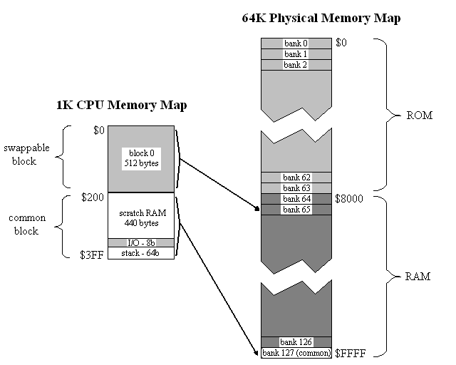
With its 10-bit address bus, the CPU sees 1K of memory. This is divided into two 512-byte blocks. Block 1 contains the stack, I/O ports, and a scratch RAM area. It is the “common” block, and is always present in the CPU’s address space no matter what is happening with bank switching. In contrast, block 0 is a swappable memory area, and can be mapped to any bank in physical memory.
Physical memory is 64K, and is divided equally between ROM and RAM. The 64K physical memory space is partitioned into 128 banks of 512 bytes each. Any bank can be mapped into block 0. Bank 127 is always mapped into block 1, the common block.
The bank select register is part of the memory-mapped I/O ports in common memory. To swap a bank, the CPU only needs to write the new bank number to the appropriate address.
A few benefits of this bank switching design are:
- Upon reset, bank 0 is mapped to block 0. That puts 512 bytes of ROM, 440 bytes of RAM, the I/O ports, and the stack all in the CPU’s address space. That’s plenty for many small programs, and means they won’t have to bother about bank switching at all.
- Larger programs (lots of program code) can be accommodated by bank switching code segments in/out of block 0, all operating on common data in block 1.
- Programs operating on large data structures can copy some bank-switching helper code to block 1, then swap additional RAM banks in/out of block 0.
- Arguments can be passed on the stack to ROM helper routines in other banks, because the stack is in common memory.
- All of ROM is addressable, with no holes. This makes storing images, audio samples, and other data in ROM much easier.
- There is no difference in handling between ROM and RAM banks. A program running entirely from RAM works just like one whose code is in ROM.
Hardware
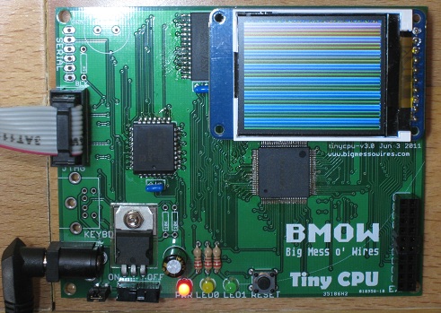
A custom-designed circuit board holds the Altera Max II EPM570T, 512KB Flash ROM, and 32KB SRAM that form the heart of the computer. A 1.8-inch color TFT on a breakout board serves as the display. A piezo speaker and two LEDs provide opportunities for simple I/O. Headers for JTAG, serial, and a PS/2 keyboard enable connections to other devices or a PC. Because the serial interface and keyboard operate at 5V, a 74LVC08 is used to level shift to 3.3V for communication with the other components. A 20-pin expansion header exposes unused Max II pins to provide additional I/O opportunities.
21 comments21 Comments so far
Leave a reply. For customer support issues, please use the Customer Support link instead of writing comments.
I can’t believe nobody has posted yet!
You’ve got an interesting project here, and it’s well-documented to boot! Keep it up.
Hi,I’m insterest in the Tiny CPU,and want to learn the cpu architecture from the Tiny CPU.
I have already readed the source code several time.but the detail of the instruction set of Tiny CPU is hard to understand by the code.
Would you please give me some documentations about the instructions set and the design of it.
Thanks a lot~~~^^!
If you’re interested in the microarchitecture, see this post: http://www.bigmessowires.com/2010/04/18/tiny-cpu-architecture/
If you’re interested in the instruction set from a programmer’s perspective, then you’re right, it’s not really documented. It’s a lot like the BMOW instruction set (which is a lot like 6502), but with many instructions and addressing modes omitted.
Once I finish my current project at work, I hope to have enough time to return to Tiny CPU and finish it.
Great projects Steve,
Loved the BMOW1 and look forward to TinyCPU or anything you come up with.
For myself been looking at Bitcoin generating architecture models. There must be a more efficient way than running multiple power hungry GPU’s? Actually there is, FPGA’s and you may be the man to get your head around programming one to act as a Bitcoin hasging core.
BMOW 1 was quite cool. I was inspired to get my CPLD-based machine on the web, too. I’m in the process of documenting it and moving all the web stuff over to a real hosting provider so I can get it into the Homebuilt CPU ring.
You can find it at:
http://sites.google.com/site/zmetzing/home/toro-clock-project
http://www.praxibetel.org/toro/toro.html
The Toro Clock Project site moved. In case the old redirect dies, here’s a new link.
Yup, I forgot to update that link! Thanks, Joe.
I hope to see many others doing their own designs, discrete logic or programmable, in the future. There’s nothing quite like the thrill of watching your CPU execute opcodes that wouldn’t run on any other existing machine.
Hey, I remember doing a “tiny” RISC CPU in an Altera device for my senior design project back in ’98! It had 16 instructions, eight in the ALU, and 8 non-ALU instructions. I targeted an EPM9320 that Altera provided to me as a sample. It was supposed to be an 8-bit CPU, but it wouldn’t fit in the 9320, so instead of paring down the instruction set, I “scaled” it down to a 4-bit proof of concept. Actually, my concept was to prove that it could be scaled upward, but ironically I ended up scaling it down. I actually utilized 98% (Yes, ninety-eight percent!) of the CPLD. Typical utilization was around 80% back in the day, but the 9000 series CPLDs had a cool feature where you could split the register bits from the and/or tree. This worked out well for a CPU design as a CPU design has a large need for both register banks and separate muxing logic for the internal busses. I still have the proto board I made using a toner transfer system. I drew the board pure art style (No auto routing tools) in Adobe Illustrator 7 on a Power Macintosh 7200. I had a ribbon cable running to a breadboard with RAM and ROM to run a simple program that exercised all of the instructions. A visible only under microscope PCB trace bridge between two “Reserved” pins kept the thing from working properly and it took me two days and the stereo scope at my intern work lab to figure out that problem. Then when I was demoing it to the professor on the day Grades were due(one hour before the deadline), the LabMate I was using to generate one-shot clocks from a spring loaded toggle switch kept double-clocking and skipping instructions, which made the prof question my design. After trying to debounce with capacitors didn’t work, we finally ran a 1Hz oscillator into the clock to prove the issue was not in my design. At the end of it all, my professor was like “That’s all you can fit in an FPGA? I’m not impressed!” Still, I got an A+ after all the hassle and got to graduate 🙂 Sorry to regale you all with my tale, but the tiny CPU project fired a neuron of projects long past 😉
buenas amigo muy interesante tu proyecto,me gustaria saber si algunas ves has desarrollado un motor grafico propio 😀 grasias de antemano
hola me gustaria saber si puedo usar los componentes elctronicos de un playstation 1, en la contruccion de una pc homebrew,tales como el procesador y cosas haci 😀
Nice project!
I wonder how much logic is avaiable in a CPLD, could this design be extended to 32 bit cpu’s?
Did you need to trim down because of logic element constraints?
Exactly. A CPLD typically only has a few hundred macrocells (logic elements), so the challenge was to simplify the CPU to fit that constraint. With a large CPLD or an FPGA, you could make a more full-featured CPU with a larger address and data size. The OpenRISC softcore CPU is one example: http://opencores.org/or1k/OR1200_OpenRISC_Processor
Pretty cool!
How does STA imm (opcode $15) work? Does it cause some kind of twisted self-modification, like on the 6800?
I would try to figure it out myself, but I can’t read Verilog yet.
Thanks,
Mike
Hey, that is an excellent question! How the heck did STA imm get in there? It makes no sense – I’m not sure what I was thinking. Looking briefly at the Verilog, I think it might treat the last 10 bits of the instruction as both an immediate value and an address in which to store it.
this is pretty cool. i can’t belief that I/C has all this in it!!!!!!!!!!!!!!
Tiny Device implements bank switching,
address decoding,
a PS/2 keyboard interface,
serial input and output,
a parallel LCD driver,
tick counter,
clock division,
a general-purpose parallel port,
and an I/O status register.
sick… i’m thinking i want to go this direction… might give the mac hobby a break. there is just so much for me to learn here.
is there a youtube video of this going? this thing is cool as hell…
ITs got all the goodies.
Did you ever get more then stripes on the screen?
hi do you have the HW’s sch & brd files and share with us?
They’re not in the file archive (see link above), since the focus is really on the CPU and not the experimental board that uses it. If you really want the board files though, I can dig them out and send them to you.
I wonder if a simple interrupt facility could be implemented while keeping the CPU below 500 macrocells. I am thinking that the single interrupt could be enabled and disabled with two simple instructions and the return instruction can delay interruption by one instruction cycle. An interrupt would result in the injection of a CALL instruction to the start of scratch RAM upon the next fetch.
Scratch the delay after return idea.
When the CPU is executing an ISR, a flag could be set to prevent interruption during the execution of an ISR. Using an IRET instruction, the CPU could then reset this flag and return from the ISR.