

Backcountry Logger v1 PCB
 Hooray, the v1 Backcountry Logger boards have arrived from the PCB manufacturer! This time I used Dorkbot PDX, and the elapsed time from the ordering cutoff date to board delivery was only 12 calendar days. For $5 per square inch, with three copies of your board, and free shipping in the USA, I call that a pretty good deal.
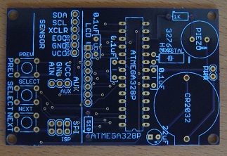
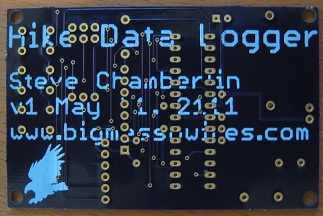 The boards have dark purple soldermask, with gold plating. The quality looks good. When I received them, the boards originally had several small tabs around the edges from the panelization process. These were easily broken off with a pair of pliers, but you can still see some slight rough spots on the edges where the tabs were.
Before I even begin to stuff the board with components, let’s count all the mistakes I already see. You can’t learn without making mistakes, and I sure made a few here.
- silkscreen layers– I delivered an Eagle .brd file for manufacturing, and I thought the silkscreen would include only the contents of Eagle’s tPlace layer. Instead, both the tPlace and tNames layers appear on the silkscreen, which results in a lot of unintended and overlapping silkscreen labels. Next time I’ll deliver individual Gerber files instead of the .brd file, so I can be sure what it will look like.
- silkscreen on pads – You can’t just run silkscreen text right across the pads… what was I thinking? Wherever text overlaps a pad, the text disappears. This makes the text on the bottom side with my name and date very difficult to read..
- text proofreading – The date text says “May 21, 2111”. It’s from the future!
- no ground plane – I forgot to include a ground plane. Fortunately with this simple, low-speed design it’s probably OK without one, but its omission was not intentional.
- untented vias – I meant to tent the vias (cover them with soldermask), but I forgot. With tented vias, they wouldn’t stand out so much, and text running on top of vias would be much more legible.
- narrow pad holes – Some of the pads have what appear to be very narrow holes. It’s tough to see in the photo, but the holes for the ATmega and the capacitors are substantially narrower than all the others. Of course the hole sizes comes from the part footprints, which I just took from the Eagle library, but it’s my fault for not checking them. I did a quick test fit, and I think everything will still be OK with the narrow holes, but it’s tight.
- insufficient part clearance – I kind of assumed that parts would exactly match their outlines in the library, but a few are bigger. The battery holder in particular is a bit bigger than its outline, enough so that it partly blocks the power jumper (right-center), and bypass capacitor next to the ATmega.
- mounting holes too big – The four mounting holes in the corners are bigger and closer to the edges than I intended. The footprint for the hole is two concentric circles, and I’d thought the inner circle was the hole itself and the outer circle was the screw head for the matching screw. Instead, the outer circle is the hole itself, and I don’t know what the inner circle is.
- soldermask on pads – The two resistors both have soldermask covering their top-side pads. If you look closely, you can see that the 1K resistor at top-right, and 510 Ohm resistor at the bottom-middle don’t have visible pads. They’re there, but covered. Fortunately the bottom side of the pads aren’t covered, and that’s the solder side, so it’s OK. I checked Eagle, and this is how the Sparkfun axial PTH resistor footprint is designed, so it’s intentional. I can’t imagine why though– it seems like a bad idea.
Now it’s time to put this thing together. Soldering iron, here we go!
Read 6 comments and join the conversation6 Comments so far
Leave a reply. For customer support issues, please use the Customer Support link instead of writing comments.
Good post! Thanks for the information.
Quick question, though: I was getting ready to make a PCB order from Seeed (for some basic Arduino shields that I’ve put together). Is there any reason why you didn’t go with Seeed this time, instead using Dorkbot? I’m just curious, since I’m quite new to the whole PCB thing.
Thanks again for sharing the errors with us: I’m learning from your mistakes in this PCB process.
I have another order pending from Seeed, but since I haven’t received the boards yet, I can’t comment on their quality. The main drawback of Seeed for me is the delivery time. They make the boards within a few days to a week of your order, but shipping from China to the US can take 2-4 additional weeks. In practice it normally seems to be more like 2 weeks than 4, so total time is probably around 20 calendar days.
Instead of charging per square inch, Seeed uses a different pricing model where all boards under a certain size are a flat price. Their standard service also includes 10 copies of your board, instead of 3 (Dortbox PDX) or 1 (Batch PCB). If you actually need 10 copies that’s great, but if you don’t they’re just trash.
Once you know the finished size of your board, and how many copies you need, then I would suggest looking at each of Seeed, Dorkbot PDX, and Batch PCB, and see how the prices compare in your case. If the prices are similar, then I would go with Dorkbot PDX since it has the fastest total time to delivery, and there’s an actual human being you can email with questions.
Thanks for sharing this project. I am thinking of doing something similar, actually a watch for downhill skiing. I’ve learned a lot and gotten a lot of ideas following you blog.
MG, that’s a great idea! Using the same pressure sensor, you could definitely build something cool to count number of runs, total descent, average rate of descent, fastest rate of descent, and more. In my application I’m only taking a measurement once a minute, but the hardware supports many samples per second, if I recall. That should be plenty to measure your instantaneous descent rate during a ski run.
Thanks Steve! That’s super-helpful information.
The Dorkbot PDX boards look pretty good, I have to say (and it’s nice that they do 4 layer ones as well, for some extra cost– I’m not at the point of needing a 4 layer board, but it’s certainly nice to know that there’s a cheap option out there for that).
Anyway, awesome work on the projects and thanks again for the info.
At least on the prototypes, I find untented vias to be more convenient. Yes, it does mean I have to double check the silkscreen and manually reposition some of the reference IDs to avoid overlapping the vias, but in exchange I get a bunch of easily accessible test points. This becomes particularly handy on boards that are mainly populated with SMT ICs and probing a signal at the chip either requires a very steady hand or an expensive clip-on.
Even if a part is in the library with a correct footprint, you should still check and see if it’s the right footprint for you. The best footprint for minimizing defects in automated manufacturing is not necessarily the best footprint when hand soldering. (For example, with SMT ICs I like to extend the pads so it’s easier to get the soldering iron tip in contact; the default footprints tend to assuming you are using solder paste and reflow.)