

Plus Too Video and Audio
I’ve been working through the details of the video and audio systems for my “Plus Too” Mac Plus clone, and things are beginning to fall into place. Here’s what I’m planning:
Video
The Plus Too will have a VGA output for connection to a standard monitor. The video will be monochrome 1024 x 768 at 60 Hz, containing a pixel-doubled image of the Mac’s 512 x 342 frame buffer. The doubled image will fit perfectly across the horizontal, but there will be some letter-boxing vertically since 2 times 342 is less than 768.
Because the pixel clock, CPU clock, and audio sample rate in the Mac are intimately related, the choice of 1024 x 768 60 Hz video will affect the possible CPU and audio rates. The 1024 x 768 @ 60 Hz VGA standard requires a pixel clock of 65 MHz. But because the image is pixel-doubled from a 512-pixel wide original, and not a true 1024-pixel image, the effective pixel clock is only 32.5 MHz. The original Mac had a 2:1 ratio of pixel clock to CPU clock, which was a result of the 16-bit memory bus width and the 50/50 time sharing of RAM between the CPU and video circuitry. Assuming the same 2:1 ratio, that would give the Plus Too a CPU clock speed of 16.25 MHz. That’s twice as fast as the original Mac, and not so good for building a faithful reproduction of the original. Unfortunately the CPU clock speed can’t be changed independently of the pixel clock without changing either the bus width or the memory interleaving scheme.
My solution is to run the CPU at 8.125 MHz, but “double pump” the RAM during each turn of the video circuitry, fetching 32 bits per turn instead of 16. This is possible because each turn is 4 CPU clocks long, which in 1984 was only long enough for one RAM access, but in 2011 is certainly long enough for two accesses, given modern SRAM speeds. Two 16-bit reads per turn will fetch 32 pixels worth of data. With a video turn occurring every 8 CPU clocks, that’s a turn rate of 8.125 / 8 = 1.016 MHz. 32 pixels at a rate of 1.016 MHz yields the required pixel clock of 32.5 MHz. Thus the Plus Too will have a 4:1 ratio of pixel clock to CPU clock.
8.125 MHz is still about 4% faster than the 7.8336 MHz CPU of the original Mac Plus (and 128K and 512K). But it’s close enough that the discrepancy shouldn’t be very noticeable.
Audio
Including the VBLANK region, the original Mac had 370 lines of video per frame. The audio hardware had a 370 byte sample buffer, and it’s not a coincidence that those numbers are the same. At the end of every horizontal video line, the hardware fetched a single byte from RAM and used it to update the audio DAC (which was not actually a DAC, but ignore that for a moment). Since the horizontal line rate was 22.2 kHz, this provided 8-bit 22.2 kHz audio. The contents of the audio buffer were played (output to the speaker) exactly once per frame.
Since the Plus Too hardware won’t have 370 lines of video per frame, having a 370 byte audio buffer is problematic. Ideally I could change the size of the audio buffer to match the new number of lines per frame, which is 1334 lines (including the VBLANK region) for my chosen video mode. Sadly, that 370 number is embedded in the Mac’s memory map and sound routines, and realistically can’t be changed. I see three possible ways to address this:
- Read a byte and update the audio DAC after every four lines of video. That would be 1334 / 4 = 333 bytes per frame, resulting in a playback rate of 20 kHz — about 10% too slow. The slowness probably wouldn’t be too noticeable. The bigger problem would be that the entire sound buffer wouldn’t be played during a single frame. Frame-synchronized code that filled the sound buffer with the next 370 bytes of data during the VBLAK interrupt would no longer work as intended. Audio would sound oddly distorted.
- Abandon the relationship between video lines and audio samples, and just divide the frame’s time into 370 intervals, fetching audio bytes at equal intervals. This might result in an audio fetch being attempted when a video fetch or CPU memory access was happening. The audio fetch would need to be delayed until the next CPU turn, and then steal the CPU turn, forcing the CPU to wait further. With some more complicated logic for /DTACK generation to force CPU wait states, this could probably work.
- Change the address decoding scheme to map the audio buffer into a 370-byte dual-port buffer implemented within the FPGA itself. Then read 370 samples per frame from the buffer at equal intervals, as with option #2. The advantage here is that the /DTACK generation circuit wouldn’t need to change and the CPU wouldn’t be forced to wait. The dual-port buffer would make it possible for the CPU to write simultaneously with an audio hardware fetch. 370 bytes isn’t very much (most FPGAs have 10K or more embedded RAM), so this might be the easiest solution.
I spent quite a bit of time considering these three options, until I realized that I could experiment with all three simply by reprogramming the FPGA after the hardware is built. The physical hardware on the board would be identical in all three cases, so I can defer a final decision until later.
Returning to the issue of the it’s-not-a-DAC, the final question is the design of the audio output circuit. The original Mac used PWM to generate the audio signal, with the amount of time that the line was high determined by the most recent audio byte. A filtering circuit smoothed this high-speed PWM signal into an audio frequency, and attenuated it to one of eight volume levels using a 3-bit volume control. The exact circuit is here (drawn by 68kmla.org forum member H3NRY):
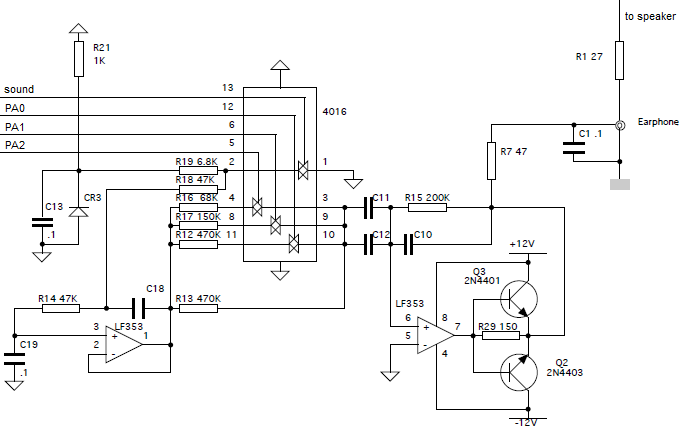
Uh… what? I see the PWM signal and 3-bit volume control coming in from the left, but everything else is lost in a sea of capacitors, diodes, op-amps, and transistors. I’m no analog guy, and I really don’t understand how this circuit works– especially the part where an op-amp drives the base of two transistors. I could just build this circuit as drawn, without understanding it, but I’d prefer to create my own solution even if the resulting audio quality is inferior. From examining this schematic, I’m unsure how much attenuation each bit of the audio volume is supposed to produce, but I could probably measure that experimentally from a real Mac Plus, or just make up some values that work well subjectively. There are a few Arduino how-tos for PWM audio that could serve as a starting point, or I could simply use a real hardware DAC.
Read 9 comments and join the conversation
9 Comments so far
Leave a reply. For customer support issues, please use the Customer Support link instead of writing comments.
Once you have an FPGA, it gets simpler.
You can generate the final PWM signal directly,
and also adjust it internally for volume. The external circuitry can then be a simple RC low-pass filter. Google pointed out this page: http://www.fpga4fun.com/PWM_DAC.html
Sigma/Delta DACs also seem popular for audio output.
The 4016 is a quad analog switch. All inputs are buffered by this switch.
If sound is high, pin 2 is connected to ground via the switch. If sound is low the signal at pin 2 it pulled high via R21. I’m not quite sure what C13 and CR3 are for, my best guess would be clamping and transient suppression.
Now follow the path of the signal from pin 2 of the 4016. It is fed to the connection between R14 and C18 via R16. The first half of the LF353 opamp in connection with R18, C19, R14, C18 and R13 form an second order active low-pass filter.
R16, R17 and R12 are parallel to R13. By switching them on and off the resulting resistance between the output of the first opamp and C11 and C12 can be varied. C11 and C12 remove the DC component from our signal and the second half of the opamp amplifies it.
Q3 and Q2 are connected in a push-pull configuration to extend the current output capability of the opamp circuit. R15 is the feedback resistor of the amplifier.
R7 and C1 form a passive low-pass filter further attenuating undesired high-frequency components.
If the above contains some errors please correct me. Useful information on opamp circuits can be found in Ron Mancinis “Op Amps for Everyone”, which can be downloaded for free from the TI website.
This schematic could use a few more labels. R21 is connecting to the +12 supply and CR3 is a 5.1 V zener diode. So R21, CR3, and C13 are forming a crude 5 V regulator. It’s not a very good regulator, but it’s inexpensive and provides an output that is free from all the switching noise that’s present on the 5 V supply used by all the digital logic circuits.
The digital signal “sound” also has residual noise from the digital 5 V supply, so instead of using it directly, it controls one of the analog switches to either ground the input of R18 or let it be pulled high by R19. It’s still the same digital “sound” signal that it started with, but this way it’s been freed of the noise in the digital supply.
Ferdinandkeil has a good analysis of the rest of the circuit. In addition to filtering with C1, I suspect that R7 also acts to protect the push-pull transistors in case of earphone short (cables and connectors can be subject to a lot of abuse).
The schematic has the + and – labels backwards on pins 5 and 6 of the LF353: pin 5, the + input, is grounded and pin 6, the – input, connects to the incoming signal and the feedback path.
PA0..2 actually control the gain rather than attenuation. The parallel resistance (Rp) of R16, R17, R12, and R13 is 470K (PA=000), 235K, 114K, 92K, 59K, 53K, 43K, or 39K (PA=111). The overall gain is 1+(R15/Rp) which is 1.43, 1.85, 2.76, 3.18, 4.37, 4.79, 5.70, or 6.13 depending on PA. To avoid clipping there would have to be some attenuation earlier, probably by R14, R18, & R19.
Erik is right, CR3 in connection with C13 and R21 form a voltage regulator. Correct me if I’m wrong, but the digital signal sound will be inverted by this circuit. If sound is high, then a connection is established between pin 1 and 2 of the 4016, effectively pulling the signal at pin 2 to ground.
Oops, I missed this inversion. Luckily the phase doesn’t matter much here.
That makes a lot more sense now. Thanks for the audio analysis guys!
Just a quick observation: The lower of the two transistors that act as a current amplifier on the output of the op-amp, Q2, is wrong. If it’s a 2N4403, then that’s a PNP type and should have been drawn with the emitter arrow facing the other way. An NPN transistor (as drawn) will not function in that circuit.
I noticed the same thing, but wasn’t confident enough to be sure if it was correct or not. This schematic was made from the original hand-drawn one, and it looks like a couple of mistakes crept in.