

Managing Multiple Power Supplies
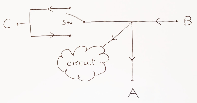
I’ve been investigating ways to handle multiple supplies and consumers of +5V 500mA power in a single project, and it’s surprisingly complicated. My circuit may have up to three simultaneous external connections: a device needing +5V power at “A”, an external +5V supply at “B”, and something at “C” that might either supply +5V power or need +5V provided to it, depending on what mode the circuit is operating in. Any of these three could be present or absent, and the external +5V supplies could possibly be connected but turned off and not delivering power.
The simple solution would be to directly connect all of those +5V lines within my circuit. That would work, and maybe it’s what I’ll do, but it presents some risks of unintended current backflow into a supply. Imagine if B and C are both connected, with C configured as a supply. If one is turned off, the other would feed +5V into it. Depending on what that supply is and how it’s designed, feeding external +5V back into a device that’s turned off may cause weird behavior or damage. A similar problem could arise if a poorly-designed device on A actually powers the +5V line instead of drawing power from it, because it has batteries or an independent supply of its own.
I’m willing to handle the bidirectional nature of C with a physical switch. But I still need something that ensures current only flows in the intended direction in/out of A, B, and C, as shown in the diagram above. The ground connections aren’t shown, but they are all tied together. Current direction arrows mean diodes, right? I think diodes would theoretically work, but probably aren’t the best choice. A diode would cause a substantial voltage drop between the supply and whatever it was powering, and you need a diode that’s physically large in order to handle significant amounts of current.
A better solution might be a transistor. From studying similar circuits, a good choice might be a power MOSFET. These have a very low resistance when switched on, resulting in only a small voltage drop. A small-sized MOSFET could also handle all the 500mA current I need for this project. But I don’t have any experience working with single MOSFETs in this kind of application. I get a bit bogged down in discussions of N and P type, enhancement and depletion, high-side and low-side switching, and so forth. I’m not completely confident I’d know which specific MOSFET to select for my purpose, and how to connect it in the circuit, and what limitations or unexpected behaviors it might have.
An even better and simpler solution might be a power distribution switch IC, like the Microchip MIC2005A. This is basically a MOSFET, but one that’s designed for this specific purpose, with some extra features like soft start, current limiting, and thermal protection. And in the SOT-23 package I’d likely use, it’s not much more expensive than a generic MOSFET.
Power distribution ICs are designed to conditionally enable a power supply, and they have an /ENABLE pin to determine when to energize OUT from the supply at IN. But I would be using them always enabled, just to get the reverse current protection feature. Maybe that means this is the wrong tool for the job, and a different solution would be better?
A second question is whether a power distribution IC like the Microchip MIC2005A actually provides reverse current protection. It has terminals labeled IN and OUT, but it’s not clear if anything prevents current flowing from OUT to IN if OUT is energized by something else. I skimmed the datasheet, but couldn’t find any mention of this.
A final question is whether connecting the OUT terminals of several MIC2005A chips would cause problems. That’s what I’d need to do, if both B and C might function as +5V supplies. I can imagine this might cause a problem if one of the MIC2005A chips finds its OUT terminal at +5V even though its IN terminal is at 0. Or it might be a problem if both B and C were turned on at the same time, both delivering “5 volts”, but one was 4.9V and the other 5.1V. I didn’t see anything in the datasheet that addresses this either.
I’m trying very hard to keep the total cost of this solution low, like 50 cents or less. There are more complex power management ICs that might simplify things, but cost $2 or more apiece. Add the cost of assembly, and a retail markup sufficient to get acceptable margins, and the final sales price of the product would have to be increased by an unacceptable amount. I would probably choose to eliminate functionality instead, or just use the “connect all +5V supplies” approach, before I made a significant increase in product price just to support power management.
My diagram shows five current direction arrows, so potentially I would need five MOSFETs or MIC2005As. But I don’t actually need one on the line to the “circuit” cloud, because there’s no possibility of current flowing the wrong way. And the two arrows at C could probably be collapsed into a single arrow, if I used a DPDT switch that reversed the connections to the MOSFET or MIC2005A terminals. And I maybe don’t really need the arrow at A. If a device at A were to backflow +5V power, it would turn on the circuit, and possibly also supply power to C depending on the switch setting. That would be unexpected, but I don’t think it would harm anything. Applying all those simplifications, I might be able to get away with as few as two MOSFETs or MIC2005As, squeaking under my arbitrary $0.50 budget.
Read 21 comments and join the conversation21 Comments so far
Leave a reply. For customer support issues, please use the Customer Support link instead of writing comments.
Whoops, I found this in the MIC2005A datasheet: “Since the switch is bi-directional when enabled, if VOUT is greater than VIN, current will flow from VOUT to VIN.” So a MIC2005A is not going to work.
Have a look at “ideal diodes” from TI and Linear. Eg. LTC4358.
Seconding LB9MG, “ideal diode” is the search term you want. Linear and some others have application notes on doing this sort of thing.
Thanks! I think I’d seen that before somewhere. All the Linear ideal diodes seem to have a minimum voltage requirement of 9V though – what’s up with that? I need something that can work at 5V. At around $3, it may also be too pricey for this project.
I thought the multiple IN pins of the LTC4358 were for OR-ing together different power supplies, but now I think they’re tied together internally, and you’d actually need a separate LTC4358 chip for each supply. That definitely rules it out cost-wise, unless I’m missing something.
The TPS22929 looks like it might work. It’s similar to the MIC2005A but it does have reverse-current protection. $0.52 in small quantities.
Argh. The TPS22929 load switch (and similar ones with reverse-current protection like SIP32510DT and AP22802) won’t work either, because it incorporates a load discharge resistor on the output. Whenever the device is disabled, it inserts the equivalent of a 100 ohm resistor between the Vout terminal and ground. This makes sense for discharging any capacitors in a de-powered circuit, but it make it impossible for another source to power the circuit instead.
Steve, have you considered Schottky diodes? they have a very low forward drop, and at 500 mA max, that should be no problem.
Yes, Schottky diodes might work. The forward drop would be around 300-400 mV, so downstream USB devices would receive about 4.6V instead of 5V. That would probably be OK, but seems a little dodgy. But if I had B powering C (from the diagram), there would be two voltage drops and the device at C would receive about 4.2V. That still might be OK, but is pretty far out of spec. It definitely meets the simple and cheap requirements, though!
The USB 1.1 spec allows Vcc to drop down to 4.40 V at the USB connector, but requires at least 4.75 V at the connector for full functionality. (Chapter 7.2.2 “Voltage Drop Budget”)
Getting rid of a Vcc star point also avoids one diode drop: Use one diode from every voltage source to supply the controller, and one diode from every voltage source to any other load.
Also, Schottky diodes drop only about 100 mV for low currents. So, you should be able to stay within the USB spec.
Well, if you can locate power supplies with a bit of adjustment in them, you can compensate for the 1st diode drop (supply B in the diagram above). Note: if you check several power supplies, you’ll probably find some that are a bit on the high side anyway. That will minimize the effect of the diode.
Then it just depends on what kind of device device C is.
Note: the lower limit for USB devices is around 4.6-4.7 volts. Much below that and you’ll start getting dropouts.
If you want to give me some more information on what you’re trying to do, I’ll try to direct you in the right direction.
Thanks both. Good point about the star configuration. This is a theoretical design for the USB-ADB converter described in my earlier post, so A would be a USB Host port, B a USB device port, and C an Apple Desktop Bus port. It gets complicated, because C could either have an ADB computer providing power, or ADB devices requiring power. B could simply be used as a source of standby power when the computer at C is off, or could be an active USB connection if A isn’t used and there are ADB peripherals at C.
I need to provide up to 500mA for USB or Apple Desktop Bus peripherals, and from my look at some datasheets, that would mean a Shottky diode drop of around 350 mV. Am I looking at this wrong? Here’s an example: https://toshiba.semicon-storage.com/info/docget.jsp?did=9019&prodName=CUS08F30
Steve, you’re right on target here. 350mV is just about right. The star configuration that Tux2000 suggested will help (good suggestion), if you need it.
If we know what some of the devices will do when applied power “backwards”, it will help reduce the number of configurations to consider.
Question: on the ADB port, do you have any idea what the computer would do if it was provided power that it didn’t generate? If not, the switch would also allow you to control things.
For the B port, would that be another computer, or is it a USB power supply? If it’s a power supply, it should get a bit simpler. Most USB power supplies that I have looked at internally would not be too bothered by voltage being applied to them. They will draw some current (as many have power LEDs), and will draw a bit more if you go above their set voltage (think zener in series with limiting resistor in series with the LED of an Optical isolator).
If a turned-off computer on the ADB port were provided 5V that it didn’t generate, it would try to run the computer, at least for one model I looked at. I didn’t try it, but the schematic shows the ADB +5V is connected through an inductor to the primary 5V supply for all the ICs.
Steve, if you are looking for cheap then a sub 1A P-Channel Mosfet for each input is the way to go. Your initial requirements were understandably vague so I am making the assumption that you want your device to receive power as long as one *or more* of the 5V inputs are live and providing power. A quick check of Mouser shows a reasonable selection of surface mount devices in the sub $0.10 range with a quantity of 100 so any production run would be much lower per unit.
I found a doc on the Infineon web site with a terrible url so Google “Reverse Battery Protection by Marco Pürschel. Application Note, 2.0, June 2009” and it should be the first link.
Another crazy idea for you, how about switching to a 3V solution so you can use cheap diodes and ignore that Vf drop? I am actually looking for a small/cheap smd diode with a 3v or better Vf at 60mA load. Space is a major consideration so I can’t just slap 4-5 signal diodes in series, although I may need to make that work.
Thanks Steve. The trouble with a high side p-channel MOSFET is that it doesn’t provide the reverse current protection I need, to prevent backfeeding current into one of the computers/supplies when it’s switched off and something else is providing power. As long as Vgs of the MOSFET is negative, the MOSFET will turn on and current can conduct in both directions between drain and source. These are more complex circuits similar to this that use some type of voltage comparator to turn the MOSFET on and off. I think that’s basically what the TPS22929 is.
I am using 3V parts for my “circuit” cloud in the diagram, but the USB and ADB peripherals at A and C demand a 5V supply, so there’s unfortunately no way around that.
After beating my head against this for a long time, I think the options here are:
1. Just don’t worry about reverse current protection. Educate the user, caveat emptor, etc.
2. Use Schottky diodes, and hope that the lowered ~4.6V remaining doesn’t cause malfunctions of USB and ADB peripherals
3. Use a combination of more expensive power mux and switch ICs
Steve, if the USB power from B comes from a USB power supply, then you should be OK on that side. The only issue then would be the ADB port. As it can’t handle receiving power (if it’s a computer), maybe the switch is the best solution.
Consider using a larger Schottky diode, for two reasons:
The CUS08F30 has an abs. max. rating of “just” 800 mA. It will burn if it has to supply two hungry USB devices, each drawing the allowed 500 mA.
Larger diodes drop less voltage. For example, the Infineon BAT60A drops 0.12 V at 10 mA, 0.2 V at 100 mA, 0.3 V at 1000 mA. Plus, it has an abs. max. rating of 3 A.
http://www.linear.com/solutions/7203 explains another trick with MOSFETs: connecting two MOSFETs with gate and source wired in parallel prevents reverse current from flowing through the body diodes.
How about two p-channel FETs in series? Tie them source-to-source sources together and use the drains as the switched terminals, so the parasitic diodes are in opposite directions. Drive the gates together so it functions like a single switch. RDS(on) will be doubled, but if that’s a problem you can get bigger FETs.
Tux2000, I didn’t follow you at first, but I think we’re talking about the same thing.
A bit late, but have you played around with constant-current diodes? I don\’t know of a mosfet version, but it should be quite doable, and the normal ones are just a jfet and a resistor rigged up so that the gate and drain are seen directly, and the source sees the gate through the resistor. I don\’t think these are normally rectifiers, but if you hide the gate behind a diode, and force the transistor off with a second resistor then I believe you\’ll get that result. Then you just need to adjust values until the passed amps are way above your needs, and you should be set.