

Spot The Design Error
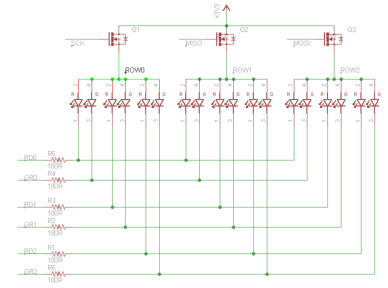
A prototype for the latest Star Ring. Q1, Q2, and Q3 use this N-channel MOSFET. The circuit runs from a 3V battery. When one of the transistors is turned on, the six red/green LEDs in the associated row can be turned on or off using six microcontroller outputs. At least that’s the theory. I built this, and it works – barely. The LEDs are extremely dim. Why?
Hint: what gate voltage is needed to turn on the transistors?
I’m not sure if there’s any way I can patch this, without having to redesign a new board.
Read 8 comments and join the conversation8 Comments so far
Leave a reply. For customer support issues, please use the Customer Support link instead of writing comments.
Well you could solder P channel fets upside-down and rotated to put gate, drain and source in the right place. I haven’t done that in a long time but from experience, that package is fairly easy to solder on upside-down if you were stupid and and swapped gate and source. At least you only have three on this board.
sounds like you need a FET with a lower gate voltage – and you can drop the LED resistors entirely, button cell can’t dump enough current to hurt the AVR or the LEDs
The circuit was originally a low-side switch, with the MCU sourcing current and the transistors enabling the connection to ground. I later reversed the circuit, but forgot to consider the impact on the transistors. P-channel FETs should work here, except to salvage this PCB I would also need to swap the positions of drain and source. That will require some kind of rotated or upside-down soldering like Alex suggested. I don’t think N-channel FETs can work, no matter what their Vgs threshold, because if the circuit works as intended Vgs will be zero (the rows will be pulled up to 3V). The resistors aren’t for LED protection, but rather to limit the current enough to get reasonable battery life from the 3V button cell.
Change the MOSFETs to BJTs?
Have a look of the figure 4 of the datasheet for the DMN63D8LW.
As you can see, near the 3,3V for the Gate potential, you are juste between 3 and … infinite Ohms
for the drain-source résistance. Where? Hum… somewhere above 3 Ohms.
In fact between 3 and 13 Ohms for VGS = 2,5V, or 10mA (see the Electrical Characteristics chart).
With 180R and 10mA, the LED are connected at 3.3-1.8V = 1.5V in téhorie.
In fact, the probleme is perhaps the LEDs…
Try to reduce the resistances to 150 Ohms…
How many PCBs did you make?
The Pfet is the way to go, yes you need dead bug mounting to put the gate in the right pad, or maybe depending how your Vgs ends up being biased you may be able to make it work by rotating the Pfet in place to get the gate at the right position (with 3 pin SOT23-3 it works).
I’ve ordered new PCBs designed for a P-channel MOSFET. I gave up on the idea of salvaging the boards with the flawed design, as there’s only three of them and it’s not critically important. I can wait the two weeks needed for the new boards to arrive.
Yeap I have made this mistake once before, but in an h-bridge circuit.
In order to use an N channel as a high-side switch the gate voltage has to be referenced from the source, now luckly they make a mosfet driver which can actually do just that using source as the reference, and some sort of charge-pump.
But its only useful in high current situations like H-bridges or class D audio.