

Archive for the 'BMOW 1' Category
First Simulation
It simulates! I completed the Verilog description of the machine, and after fixing one place where I’d used an active high instead of an active low enable single, it worked like a champ. I implemented the microcode for NOP, JMP (absolute), and HALT. I was able to run this simple program from ROM: NOP
LOOP: NOP
JMP LOOP
Of course I don’t actually have an assembler or any other software tools, so I couldn’t write the program symbolically like this. My test program is just a bunch of hex numbers entered by hand into a text file. That’s marginally tolerable for a 5-byte assembly program, but writing microcode that way gets old very, very quickly. Each line of microcode is 24 bits wide, and keeping track of what every bit means in my head, for every line of microcode in even a simple instruction like JMP, is near impossible. I need to write a quick-and-dirty microcode assembler before I go any further.
Here’s a simulation trace of the machine booting up and executing the above program.
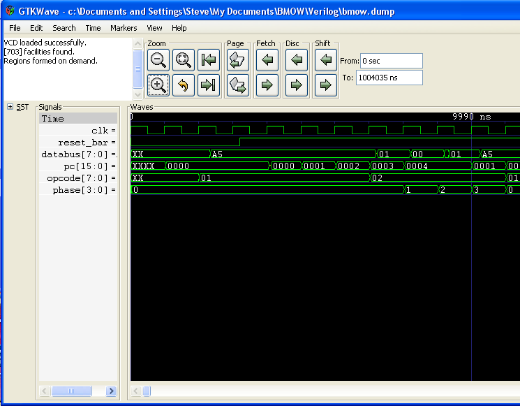
I used the awesome free tools Icarus Verilog for compiling and simultating, and GTK Wave for analyzing the waveform results. I put basic timing information into the hardware model as I was constructing it, using Verilog delays to make outputs lag inputs by the worst-case propagation delay cited in the datasheet. Theoretically, I should be able to use this to determine a lower-bound on the machine’s clock speed: just crank up the simulated clock speed until it stops working.
While completing the Verilog description of the machine, I found that I needed more “glue logic” chips for computing simple boolean functions than I’d like. Decoding memory addresses to enable the appropriate memory-mapped hardware required three different chips, and I needed several more to help with hardware initialization signals during reset. I ended up needing at least one each of NAND, NOR, AND, and OR. If I were more clever, I think there’s a lot of opportunity to clean up this logic and reduce the required chip count. Maybe I should look at using a PAL (or PLA? are they the same thing?) to compute all my simple boolean functions on a single chip, although it might be a lot slower.
I had an idea for a way to add a Y register to the machine, with just two more chips: a ‘377 register and a ‘244 driver. The obvious place to add it as at the right ALU bus, where there are presently only 3 inputs, but the control ROM encoding allows for 4. The problem is that the control ROM only allows for 8 “load destinations”: A, X, T, PCLO, PCHI, ARLO, ARHI, MEM. My idea was that I could have ARLO chain-load from ARHI instead of from the data bus, with just a single load enable signal instead of separate lo/hi enables. That would free up space for a Y load enable. Of course it would mean the machine could never load ARLO and ARHI independently: it would always have to load them one after another, first ARLO, then ARHI. I’m not sure if that’s practical, and I suspect it may not be, at least not without a performance penalty.
Construction update: I’ve started looking further into how to assemble this thing. I’m planning to use wire-wrap construction, even though I have no experience with it, since it seems like that’s what everyone else does. I found some used wire wrap tools and boards on eBay, and I’ll try to pick up something cheap. I’m not sure yet what I’ll mount the board inside. Maybe an old PC case, or a vanilla plastic project case, or a wooden box. It needs to be something to which I can mount some LED displays, switches, and buttons, with a little bit of homebrew bling, even if it doesn’t look like the bridge of the Enterprise.
Read 1 comment and join the conversation6502 Inspiration
The design of my machine has been significantly influenced by the 6502, the microprocessor used in most 80’s home computers, and the one with which I’m most familiar. There are no published descriptions of the 6502 internals that I know of, however. The documentation describes the instruction set interface, not how those instructions are implemented.Still, I was able to infer a lot from the nature of the 6502 instruction set and addressing modes, and the known clock cycle requirements for the various instructions. I plan to have an instruction set very similar to the 6502’s, to make it as easy as possible to port code. That may seem uncreative or like cheating to some, but I don’t see a good reason for inventing my own oddball instruction names, conventions, and assembler syntax just for the sake of being different. So where possible, I’ll make instructions that look and act like their 6502 counterparts.
I also plan to support at least these addressing modes:
| Mode | Example | Description |
| implied | INX | operand implied |
| absolute | LDA $HHLL | operand is address $HHLL |
| absolute, X-indexed | LDA $HHLL,X | operand is address incremented by X with carry |
| immediate | LDA #$BB | operand is byte (BB) |
| indirect | LDA ($HHLL) | operand is effective address; effective address is value of address |
| PC-relative | BEQ $BB | branch target is PC + offset (BB), bit 7 signifies negative offset |
| stack-relative, X-indexed | LDA SP,X | operand address is stack base incremented by X with carry |
All but stack-relative addressing mode are from the 6502.
Despite the similarities in instruction set and addressing modes, my machine will be inferior to the 6502 in that it lacks a Y register, zero-page addressing, decimal mode, interrupts, and the capability to set the stack pointer and push the condition code flags on the stack, among others. On the other hand, it will be superior to the 6502 in that it provides a full 16-bit stack pointer (the 6502 has an 8-bit SP) and stack-relative addressing mode, which I see as a necessity for implementing programs in languages like C.
I’ve worked out the microcode and timing for a handful of sample instructions, using my proposed microarchitecture design. Here’s how I stack up against the 6502. Where two numbers are shown, the larger number is for the case where a page boundary (256 bytes) is crossed while doing address arithmetic.
| Instruction | Description | 6502 clock cycles | My clock cycles |
| ADC | add with carry, immediate | 2 | 2 |
| JMP | jump to absolute address | 3 | 4 |
| BMI | branch if minus | 3/4 | 4/5 |
| INC | increment memory, absolute, X-indexed | 7 | 7/8 |
| PHA | push accumulator onto stack | 3 | 2 |
| JSR | jump to subroutine, absolute | 6 | 8 |
| RTS | return from subroutine | 6 | 6 |
| LSR | logical shift right 1 bit, implied | 2 | 9 |
| LDA | load accumulator, stack-relative, X-indexed | N/A | 4 |
Component Details
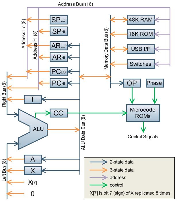
An explanation of the components shown on the block diagram I posted yesterday.
Registers:
- A is the accumulator register, although the hardware assigns it no special significance, and X can do anything that A can.
- X is the index register. It can be used for indexed addressing modes, where the value in X specifies an offset from a base address to get the effective address. It can also be used as a general-purpose register.
- T is a temporary register, used by the microcode to implement various instructions, but not visible to the application programmer.
- The pseudo-register X7 is used to sign-extend the 8-bit value of X when adding it to a 16-bit address.
- 0 is just a hard-wired 0 value.
- CC is the condition code register, which stores the flags (equal, carry, etc) from an ALU operation. It’s a parallel in, serial out shift register, so only one flag can be examined per clock cycle, and it may be necessary to spend a few cycles to shift the desired flag into position to be read. I stole this design from my college textbook.
Addressing: Any of three different sources can be selected by the microcode to drive the address bus on a given clock cycle. The low or high byte of the address bus can also drive the data bus if needed. The address registers are counters, and so can be incremented or decremented without using the ALU. None of the address registers are directly visible to the application programmer.
- PC is the 16-bit program counter, with separate low and high bytes.
- SP is the 16-bit stack pointer.
- AR is a generic 16-bit address register, used for memory accesses where the value in PC and SP can’t be disturbed.
Control: The microcode is stored in 3 parallel 8K ROMs, yielding 13 inputs and 24 outputs. The inputs are the opcode register OP for the current instruction (8 bits), the phase (a 4-bit counter, essentially a PC for the microcode), and the flag input from the condition code register. The outputs are:
- ALU left input selection: 2 bits
- ALU right input selection: 2 bits
- ALU function (add, subtract, shift, etc): 6 bits
- ALU drive enable: 1 bit
- Data load enable signals (can be one of A, X, T, PCLO, PCHI, ARLO, ARHI, MEMORY): 3 bits
- Enable CC: 1 bit
- Load/~Shift CC: 1 bit
- Address bus source (can be one of PC, AR, SP): 2 bits
- AR++: 1 bit
- PC++: 1 bit
- SP++: 1 bit
- SP–: 1 bit
- OP load enable: 1 bit
- Not connected: 1 bit
A microcde example might help.
ADC (Add With Carry): Interpret the next 2 bytes after the opcode as a memory address, read a value from that address, and add it to the accumulator, loading the CC register with the carry flag. 4 clock cycles.
| ALUleft | ALUright | ALUfunc | ALUdrive | DATAload | EnableCC | ADRsource | PC++ | LoadOP | Comment |
| x | x | x | 0 | ARlo | 0 | PC | 1 | 0 | ARlo <- MEMORY(PC), PC++ |
| x | x | x | 0 | ARhi | 0 | PC | 1 | 0 | ARhi <- MEMORY(PC), PC++ |
| x | x | x | 0 | T | 0 | AR | 0 | 0 | T <- MEMORY(AR) |
| A | T | add | 1 | A | 1 | PC | 1 | 1 | A <- A + T, LOAD CC, OP <- MEMORY(PC), PC++ |
Memory: I expect to have RAM, ROM, a combination UART/USB interface, and console switches share a single 64K address space. I plan to use a single-chip USB interface solution like this one, which should be easier than a serial port for connecting to a PC. I haven’t yet looked at it in detail, though. The exact type of ROM (EPROM, E/EPROM, Flash) is still up in the air as well.
Be the first to comment!The Adventure Begins
After several weeks of digging through the details of other designs, re-reading my college texts, sketching out data paths, and writing test microcode for my various design ideas, I arrived at what I hope is a mostly-complete block diagram for the computer. I wrote out the microcode for a dozen or so instructions that I expect to have in the machine’s instruction set, to prove to myself that they were all computable in a reasonably efficient number of clock cycles. Most instructions look like they’ll require 3 or 4 clocks, with the most complicated read-modify-write instructions using indexed addressing modes taking about 10 clocks.
One of the possible ALU inputs is a hard-wired zero. When writing the sample microcode, I found that a zero input would help me shave a clock or two off many instructions. X[7] is another special ALU input. It’s the sign bit (bit 7) of X, replicated 8 times. It makes it easy to do sign extension when adding a signed 8-bit number to a 16-bit address, such as when doing a relative jump or using an indexed addressing mode. It feels a bit ugly, but it cuts two clock cycles off every branch instruction.
Note that the ALU data bus and memory data bus are separated by a bi-directional bus driver. This enables them to do work in parallel. For many instructions, the next opcode can be fetched from memory and stored in the OP register simultaneously with the last step of the computation by the ALU.
I haven’t yet created a detailed circuit schematic, but I know roughly what parts I’ll need. I made an approximate tally of 40 chips used in the design, plus a few more I’ll undoubtedly need for clock generation, signal buffering, and glue logic. The total should be under 50 chips, which I hope is few enough to fit onto a couple of circuit boards. Physical construction is still a ways off, but I’m always trying to think ahead.
The next step is to get feedback on the current design, and make sure there aren’t any major problems I overlooked. After that, I plan to move on to creating a Verilog model of the design, so I can simulate it and work out the flaws before I break out the soldering iron.
Be the first to comment!