

Archive for the 'Tiny CPU' Category
Tiny CPU
I’ve got a working CPU! You can grab the Verilog source and a testbench here. The instruction set and addressing modes are as I described them in my previous post, except that I shrank the stack pointer to 6 bits (64 byte stack), and was able to add the missing branch if carry/zero not set instructions. The CPU has a 10-bit (1K) address space, and fits in 119 macrocells of an Altera EPM7128S, when set to optimize for area and with Parallel Expander Chain Length set to 0. Sometime soon, I’ll make some nice datapath diagrams and post them.In addition to the small address space and limited instruction set, there are a few ugly elements of the design that were necessary to make it fit the device. The absence of a Compare X instruction is glaring, but is impossible to include with significant changes. There’s also a wasted state after many of the math/logic ops, in which the Zero flag is redundantly set. This makes those instructions take one clock cycle longer than actually necessary, but was necessary to avoid more complicated state transition logic. The Zero flag handling in general is definitely awkward.So what’s next? I hope to shrink the design slightly further, by simplifying logic, using more Altera primitives, or by using a smarter instruction set encoding that uses instruction bits directly as control signals. If I can save a few more macrocells, I hope to increase the address space to 11 or 12 bits (2K or 4K), because 1K feels very limited.Beyond that, I’m considering a few larger changes:
Fixed Instruction Size
The current design has instructions that are one, two, or three bytes in size. I’m considering moving to a fixed instruction size of 2 bytes: 6 bits for the opcode, and 10 bits for an address or constant value. This would simplify the state machine logic, eliminating extra states needed to perform operand fetches, and reducing the logic resources needed to implement the state machine. It would probably also result in slightly more compact code, making more efficient use of the limited address space.The downside of a fixed instruction size is that it would also fix the address size at 10 bits (or maybe 11 if I’m really clever), with no hope of increasing it. It would also require an opcode register, to hold the first 8 bits of the instruction while the second 8 bits are fetched. And it would force me to throw out the bastardized 6502 assembler I’ve been using, and create some new software tools.
Larger Bus Size
If I switch to a fixed 16-bit instruction size, it may also be worthwhile to switch to a 16-bit data bus. This would permit loading an entire instruction in one clock cycle, eliminating the need for the opcode register, and further simplifying the state machine. The downside is that I’d then need extra logic to make the memory byte-addressable for load/store of data, or else increase the data word size to 16 bits and forget about byte addressing entirely. A larger data bus output mux would also be needed. And of course, two parallel 8-bit RAMs would be needed on the CPU board.
Harvard Architecture
Not a Colonial Period building at Harvard University, but a computer with separate address spaces for programs and data. This would permit a 16-bit interface to program memory, and 8-bit interface to data memory, which is seemingly the best of both worlds. The program memory address bus wouldn’t need a mux, because it would always be driven by the program counter. Separate program and data memories would also allow for faster CPU operation, by enabling instruction fetches and data access to happen in parallel. The total amount of addressable memory would also increase, because the program and data memories could each be 1K in size, for 2K total.Separate program and data memories mean the CPU board would need two 8-bit ROMs as well as an 8-bit RAM, further increasing the component count.The major drawback of the Harvard Architecture is that working with large data constants like strings and tables is cumbersome, because they must be loaded or copied a byte at a time using Load Immediate instructions. The indexed address instructions typically used to access such structures operate on the data memory. The standard solution to this problem is to use a Modified Harvard Architecture, adding new instructions like Load Constant Indexed to fetch values from program memory. Unfortunately that negates some of the original advantages, requiring an additional address register for program memory, an address bus mux, and additional complexity in the state machine.
Read 4 comments and join the conversationBack-Annotation
I think I’m close to having this CPU fit the 128 macrocell CPLD, but running into some problems with the final details. Soon I’m going to work on a physical board layout for this CPU, at which point all the pin assignments need to be finalized. Any further design tweaks need to maintain those pin assignments, or else they could not use the same board.Altera’s Quartus II software meets this need with a tool called back-annotation. Once you’ve synthesized the Verilog design, and computed a fit for the particular device you’re using, you can back-annotate the original design with the pin placements determined by the fitter. Then if you later change the design, the software will attempt to keep those same placements, or report failure if it can’t.That sounds great, except when I use back-annotation, it always causes fitting to fail. Starting with no constraints, I can synthesize and fit my design successfully (currently 117 macrocells), then back-annotate the device and pin assignments, and run synthesize and fit again. Since I made no changes to the design, the result the second time should be identical to the first, and should match the back-annotation constraints perfectly. But what actually happens is that the second run of synthesize and fit fails, complaining that it’s unable to pack the cells into LABs successfully. This is proving very frustrating, since it’s a showstopper problem if I can’t find a solution.
Be the first to comment!Success?
I think I’ve succeeded at cramming a decently useful CPU into this 128 macrocell device! I threw away my first design and started over from scratch, abandoning almost all the 6502-related elements, and working closer to a minimal instruction set design. I also changed the Verilog structure to explicitly specify the internal datapaths between CPU registers, rather than the more behavior-oriented design I tried originally.
The major caveat is that none of this is tested it yet. No testing whatsoever. It’s virtually certain that the design contains many mistakes, some of which may cause it to fit into fewer macrocells than it would otherwise. As of now, the design occupies 121 of 128 macrocells. Due to routability contraints, however, I can’t really make use of the last seven.
My primary goals were to making a working 8-bit CPU, with a stack, index register, and indexed addressing mode. I’ve accomplished that, but a lot of other nice stuff had to be tossed out. Here are the features that the CPLD CPU supports, and doesn’t support:
Addressing Modes
Supported: immediate, absolute, absolute with index
Not supported: indirect, indirect with index, read-modify-write
Indirect addressing would be nice, but I’m not going to lose sleep over its absence. Self-modifying code can be used as a sort of poor-man’s indirect addressing where needed.
Program Flow
Supported: jump, branch if carry set, branch if zero flag set, call, return
Not Supported: indirect jump, branch if carry not set, branch if zero flag not set, negative flag, overflow flag
The overflow flag is rarely used, and a subroutine can be written to do the same thing if needed. The negative flag would be more useful, but not critical. Branch on flag not set would be very useful, but can always be avoided by modifying the branch test.
Math and Logical Operations
Supported: add A, sub A, compare A, nor A, load/store/push/pull A, load/store/push/pull X, increment/decrement X
Not supported: add/subtract with carry-in, compare X, and, or, xor, shift, rotate, test, register-to-register transfers, direct set/clear of flags
I decided the lack of a carry-in wasn’t a big deal. You can always test the carry out, and manually add 1 to the next stage of a multi-byte addition or subtraction.
Having NOR as the only logical operation seems strange, but is surprisingly powerful:
not A = A nor 0
A or B = (A nor B) nor 0
A and B = (A nor 0) nor (B nor 0)
For the common task of AND-ing a number with an immediate value to check if a particular bit is set, this can be done with NOR in a single step if you use the bitwise-complement of the immediate value, and also reverse the sense of the test:
NOR #$7F
BZ highBitIsOne
Other missing operations can be easily simulated:
clear carry = ADD #0
set carry = SUB #0
left shift = STA temp, ADD temp
transfer A to X = PHA, PLX
transfer X to A = PHX, PLA
Of all the missing functions, the only ones I really wish I could squeeze in are the branch if not set, and compare X. Not having compare X means that any loop over X has to start at some number and go down to zero, instead of start at zero and go up. Most of the time that’s probably OK. In an emergency, compare X could be simulated as:
PHA, PHX, PLA, CMP, PLA
But that’s pretty ugly, and it also assumes that PLA doesn’t modify the flags (still undecided).
I will post the Verilog code once it’s tidied up a bit more, and I’m confident I’ve squeezed it as much as possible.
Be the first to comment!Synthesis Puzzles
The more I try to understand the Verilog synthesis tool behavior, the less I understand it. I decided to go back to square 1 with my design, and start by implementing a basic 8-bit counter that can be reset, loaded, incremented, or decremented. Here’s the source:
module counter

  (input clk,

  input reset,

  input [3:0] state,

  input [7:0] d,

  output reg [7:0] q);


  localparam [3:0] load = 4'b0000,

      inc = 4'b0101,

      dec = 4'b1111;


  always @(posedge clk or negedge reset) begin

    if (!reset)

      q <= 0;

    else if (state == load)

      q <= d;

    else if (state == inc)

      q <= q + 1'b1;

    else if (state == dec)

      q <= q - 1'b1;

  end

endmodule
If I synthesize that using Altera Quartus II v9.0, with a Max 7000S series target device (EPM7128SLC84-15), and the optimization set for minimum area, it uses 10 macrocells. 10 macrocells for an 8-bit counter. The “Timing Closure Floorplan” view will show which macrocells were used, and the equations implemented in each one. It turns out that the first 6 bits of the counter each fit in a single macrocell, and use a T-type flip-flop with four product terms each, which follow a recognizable pattern. But for unknown reasons, the software implements the last two bits completely differently, using D-type flip-flops, an extra macrocell per bit for additional product terms, and one shared expander term. If you’ve got Quartus II Web Pack installed, you can easily confirm this yourself.
I couldn’t understand why the software didn’t just follow the pattern of the first 6 bits for the 7th and 8th bits too. There didn’t seem to be any limit on number of product terms or inputs that it would run into, as far as I could tell. I decided to try it, by using Altera primitives to explicitly specify a T-type flip-flop for all 8 bits, and listing out the exact logic equations for each bit. You can view the Verilog code here: counter_v2.v
The new version worked fine. In fact, it worked better than fine. It fit in 8 macrocells instead of 10, and used no shared expanders or other magic. And it was not only smaller, it was also faster. The software computed a maximum speed of 76.92MHz, compared to only 45.45MHz for the first version.
128 Is Not Enough
With more work, I was able to further squeeze the design down to 77 macrocells! You can grab the latest version of the Verilog files here.Unfortunately, when I then started to add the X register and its related functionality, things turned ugly very quickly. Even just adding an X register that could be loaded and stored, incremented and decremented, ballooned the macrocell count to 111. I went back and forth over it several times, trying various optimizations. I even tried doing a major reorganization of the whole design, moving all the math ops to the ALU, and introducing explicit datapaths instead of relying on Verilog to infer them, but nothing helped too much. And I can’t really go all the way to 128 macrocells anyway, due to routing congestion and other constraints. Even the 111 macrocell version does not actually fit the Max 7128.I’m still going to try a few other changes to see if I can improve the resource usage enough, but I know that adding indexed addressing and a stack is going to require lots more resources, so I’d likely just be postponing the inevitable. I think I will end up with three choices:
- Be satisfied with what I have now, add a few more little things, and call it done. That would mean giving up indexed addressing and a stack, making the CPU far less capable.
- Start over from scratch with a new, detailed design that accounts for exactly how it will be synthesized. Essentially, compute by hand the logic equations that should be implemented in each macrocell, so I can know exactly what’s happening and where the resources are going, and hope to use them more efficiently.
- Drop the idea of a 6502-lite CPU, and implement some entirely different design with a simpler architecture, like a stack machine.
At the moment, none of those options really appeal to me. We’ll see…
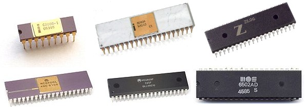
Read 3 comments and join the conversation8-Bit CPU Comparison
BMOW’s instruction set was a close cousin to the 6502’s, and so when I started on CPLD CPU, I initially intended to try something different. I looked at the Intel 8008 and 8080, Zilog Z80, and Motorola 6800 and 6809, which were all popular 8-bit CPUs back in the 1970’s and 80’s. After studying up on the architecture of all these different CPUs, I decided that the 6502 was still the best choice to use as a model, because I believe it can be implemented using the least CPLD resources.
The cross-CPU comparisons were very interesting. The key differences between these early 8-bit CPUs fell into four main areas: number of data registers, 16-bit instruction support, address registers, indexed addressing.
Number of Data Registers
More registers are just about always better, except where you’re starved for logic resources in a tiny CPLD. While the 6502 has three 8-bit registers A, X, and Y, my plan is to only include A and X in the CPLD CPU instruction set.
CPU 8-Bit Data Registers:
- 8008 – 7, ABCDEHL
- 8080 – 7, ABCDEHL
- Z80 – 7, ABCDEHL
- 6800 – 2, AB
- 6809 – 2, AB
- 6502 – 3, AXY
16-bit Extensions
While all the CPUs in this group are 8-bit designs, some support a limited number of 16-bit operations too. These are very handy for the programmer, but any 16-bit operation can also be performed as a series of 8-bit operations, so the difference is one of speed and not capability.
CPU 16-bit Support:
- 8008 – none
- 8080 – BC, DE, HL can be joined to form 16-bit registers. They support load/store of 16-bit values, and increment/decrement. Addition/subtraction of 16-bit registers is supported when HL is used as an accumulator.
- Z80 – Same as 8080, with some added flexibility on supported operations.
- 6800 – none
- 6809 – AB can be joined to form a 16-bit register D. It supports load/store of 16-bit values, and addition/subtraction/compare with a 16-bit value in memory.
- 6502 – none
Address Registers
Most modern CPUs store an address in a user-visible register, then use other instructions to manipulate the data at that address. These may be registers used specifically for holding addresses, or general purpose data/address registers, but either way the size of the register must be at least as large as the address space of the CPU. For example, the 8008 and 8080 have the M register, which can hold a 16-bit address. A byte can then be fetched from that address into the accumulator with the instruction MOV A,M. This is convenient, because you can do things like perform arithmetic on M in order to construct the right address for a value in a struct.
Another way of approaching addresses is to include them directly in the instruction itself. For example, the 6502 can fetch a byte from address $0123 into the accumulator with the instruction LDA $0123. This has the advantage that you don’t have to load $0123 into an address register first, but it means you can’t do arbitrary arithmetic on the address.
A CPU that supports absolute addresses directly in the instruction must have a hidden, temporary address register. That address in the program code has to be loaded somewhere, so that it can then drive the address bus, and a user-hidden address register fits the bill nicely.
In a CPLD CPU, the user-visible and user-hidden address registers both require space: one macrocell per bit. 10 macrocells for an address register is expensive, when your entire device only has 128. Having only a user-visible address register creates a fairly clunky programming experience, because it rules out having absolute addresses in the instruction, and forces the programmer to manually load the address register first before every memory reference. This is what the 8008 does. Most CPUs have both. The 6502 is unique in this group by having only a hidden address register, and no user-visible one. This gives up some flexibility, but is still a workable solution and eliminates one large register from the CPLD. The 6502’s zero page mode can also turn the first 256 bytes of memory into 128 pseudo-address registers.
CPU Has a User-Visible Address Register?
- 8008 – Yes, HL (also called M). ALL memory references must be done with this (no absolute addressing). Must load L and H separately.
- 8080 – Yes, BC, DE, HL. Can swap DE<->HL. Also supports absolute memory addresses.
- Z80 – Yes, Same as 8080. Adds some additional flexibility for addressing modes.
- 6800 – Yes, has a 16-bit X register. This functions like an address register when used with a absolute base address of 0. Only limited support for arithmetic with X. Also supports absolute memory addresses.
- 6809 – Yes, has 16-bit X and Y registers. Otherwise same as 6800.
- 6502 – No. Supports absolute memory addresses, and page 0 of memory as a set of pseudo-address registers.
Indexed Addressing
A very common pattern in assembly language programming is to reference a memory location using a combination of a base address and an offset. When performing some operation to many consecutive memory locations, this is generally faster and more convenient than altering the base pointer each time through the loop. For example, the 6502 can load a byte to the accumulator at some offset from address $0123 with the instruction LDA $0123,X. This takes the value currently in the X register, adds it to $1023, and uses the resulting address as the location from which to load a byte. Here’s an example 6502 programming using indexed addressing to sum all the values in memory locations $1000 to $100F:
  ldx #$0F     ; initialize X index

  lda #$00     ; register A holds sum, initialize to 0

  clc          ; clear carry flag

- adc $1000,X  ; add the byte from memory to the running total

  dex          ; decrement X index

  bpl -        ; if index is >= 0, branch to start of loop and keep going
Not all those early 8-bit CPUs supported indexed addressing. For CPUs with a user-visible address register, it’s not strictly necessary, because the programmer can accomplish a similar result by doing arithmetic on the value in the register. But even where it’s not necessary, it’s still a very handy feature. The 6502 supports indexed addressing in the most resource-efficient manner of the CPUs in this group.
CPU Supports Indexed Addressing?
- 8008 – No, must manipulate the address register manually.
- 8080 – No, must manipulate the address register manually.
- Z80 – Yes, uses two 16-bit address registers, and an 8-bit offset that’s part of the instruction.
- 6800 – Yes, uses one 16-bit address register, and an 8-bit offset that’s part of the instruction.
- 6809 – Yes, uses two 16-bit address registers, and an 8-bit offset that’s part of the instruction.
- 6502 – Yes, uses one 8-bit offset register, and a 16-bit address that’s part of the instruction.