

Z-80 Based Credit Card Terminal
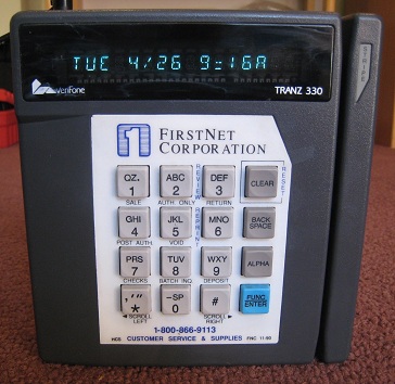 I found an old credit card terminal at an electronics surplus store recently, and bought it to tinker with. $5 at Weird Stuff in Sunnyvale! This Verifone Tranz 330 was used to process credit card transactions in the 80’s and 90’s, and is probably still used today some places. I wasn’t really interested in the credit card aspect though, but hoped to take it apart, learn how it works, and see if I could do anything interesting with it. Inside is a simple, self-contained 8-bit computer with a lot of hacking potential.
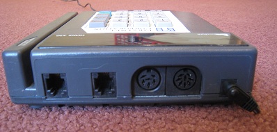
The Tranz 330 has a 16 key keypad, 16 character vacuum flourescent display (each charachter with 16 alpha-numeric segments), and a serial port with an 8 pin DIN connector. It also has an internal modem, a pair of telephone jacks, and a specialized 6 pin DIN serial port intended for use with peripherals. Lots of interesting interfaces to experiment with here.
Inside are two stacked circuit boards. The logic board contains a Z-80 CPU running at 4MHz, with a 32K socketed ROM, and 32K SRAM. The display board contains the VFD controller and keypad interface, as well as a piezo speaker.
So what do I do with this thing? It’s a full-on Z-80 based computer capable of lots of mischief, cramped only by the limited keypad and display. In theory, I could play Zork on this box. The socketed ROM would make it easy to replace the credit card terminal program with something of my own.
The challenge lies in determining the memory and I/O mapping used. How do you read the keypad? How do you write a character to the display? How do you work with the serial port or drive the speaker? I could dump the contents of the ROM and reverse-engineer the credit card program to find the answers. That’s probably the best way to go, but it sounds like a pain in the butt. I could also attach probes and examine the busses with my logic analyzer while the terminal is running. The logic and display boards are joined by a single 20 pin connector, so there’s not that much to analyze.
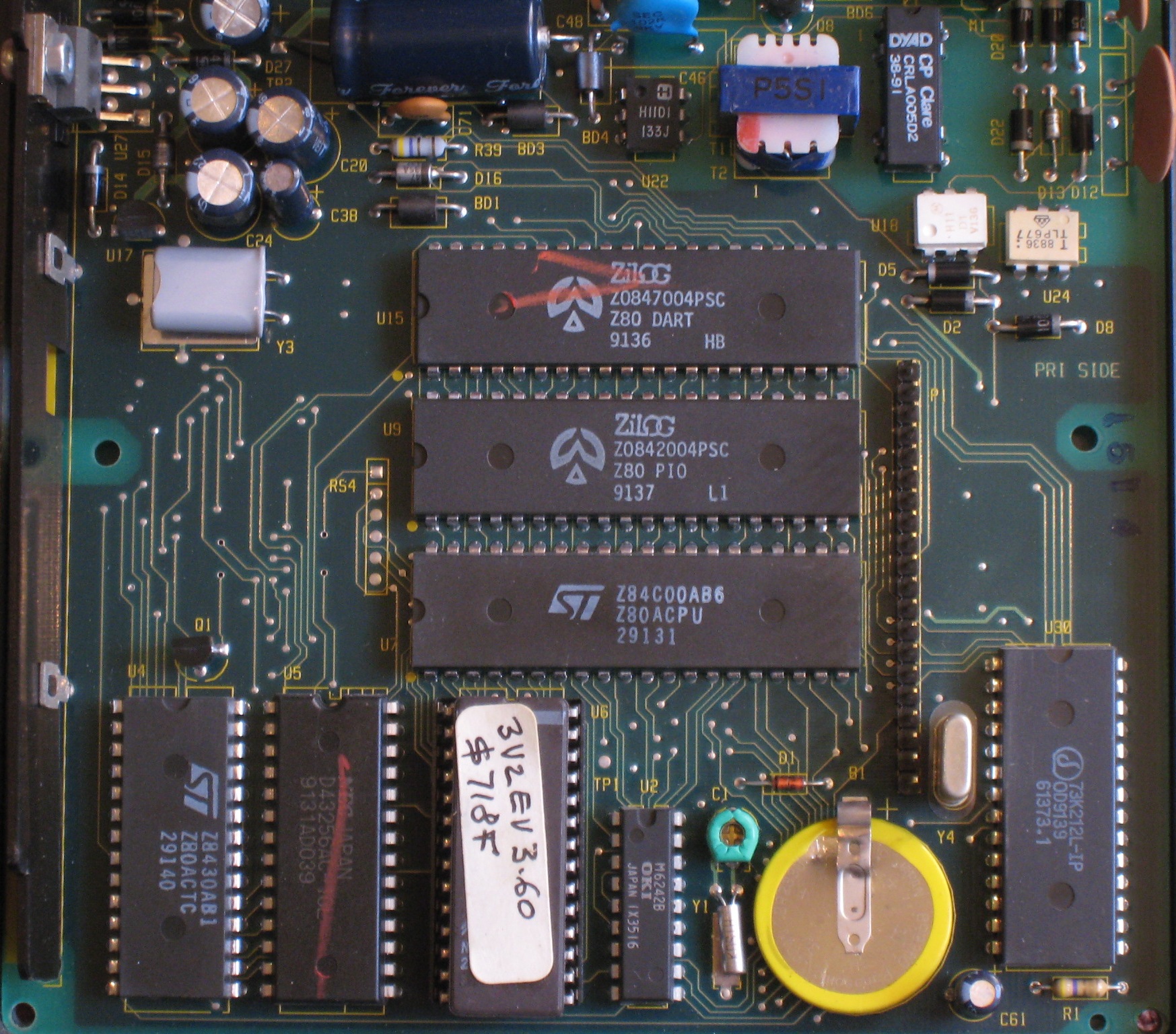
Meanwhile, let’s take a closer look at the components on the circuit boards, and see what’s there. Examining the CPU board first, in the center there’s the Z-80 CPU, PIO (parallel ports, probably used for the keypad and display), and dual UART (presumably used for the serial ports). Across the bottom row from left to right, there’s the Z-80 counter/timer, 32K SRAM, 32K EPROM, real-time clock chip, battery, and the single-chip modem. There are a few smaller chips at the top– I couldn’t learn anything about them, but by their placement I’m guessing they’re related to the phone interface.
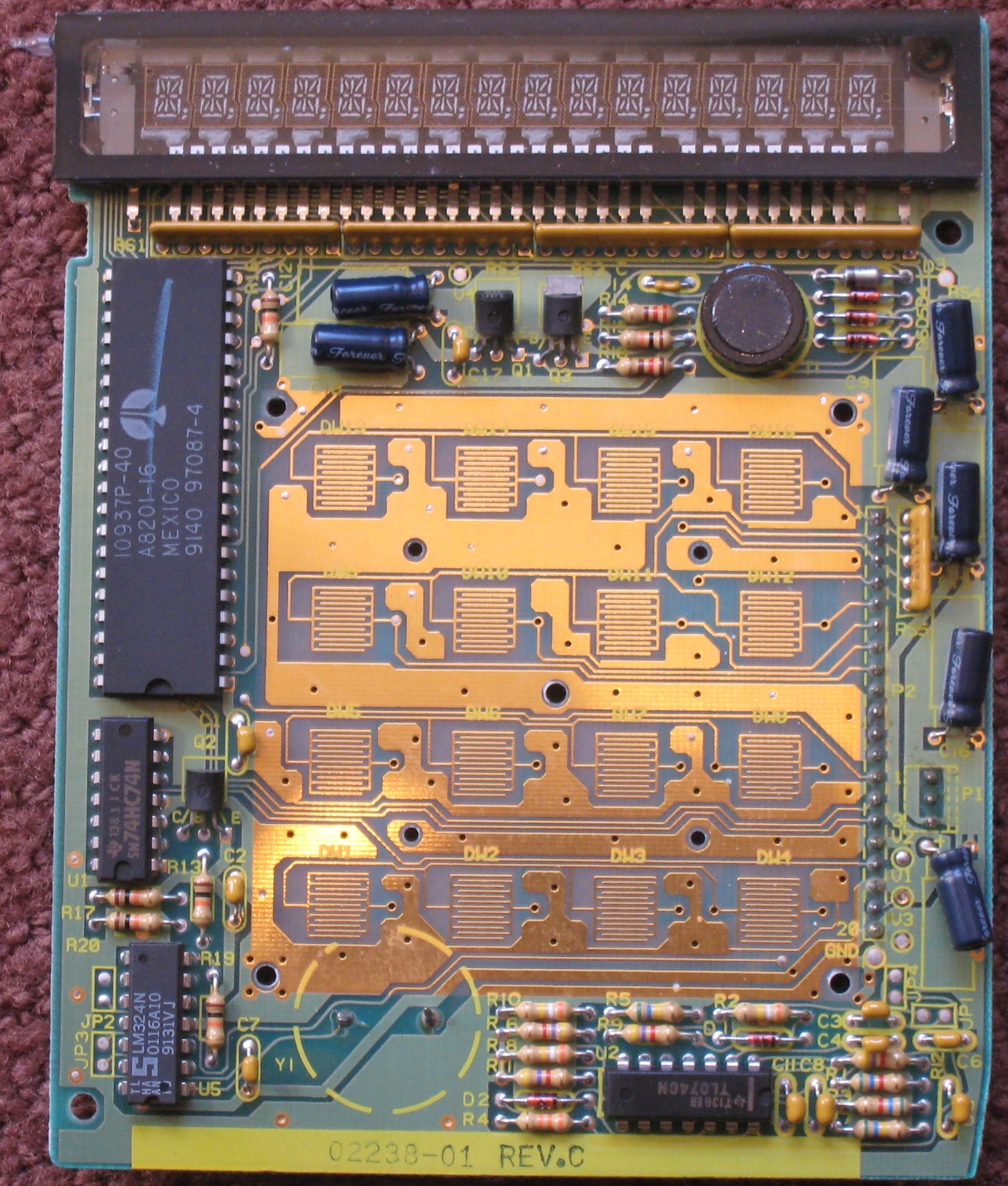
On the display board, examine the chips going counter-clockwise beginning with the largest chip. The large chip is the VFD display controller, a Micrel MIC10937. Following that is a dual-D flip-flop chip, a quad op-amp chip, and a second quad op-amp chip of a different type. I’m not sure what the eight op-amps are needed for– powering the VFD perhaps? Driving the speaker? Decoding the keypad key presses?
Post your best ideas for interesting hacks using this little box!
Read 33 comments and join the conversationTiny CPU Instruction Set
After four months of inactivity, here’s some documentation for the Tiny CPU instruction set.
| opcode |
x0 |
x1 |
x2 |
x3 |
x4 |
x5 |
x6 |
x7 |
x8 |
x9 |
xA |
xB |
xC |
xD |
xE |
xF |
|
0x |
SUB abs | SUB imm | SUB abs,X | ADD abs | ADD imm | ADD abs,X | CMP abs | CMP imm | CMP abs,X | NOR abs | NOR imm | NOR abs,X | ||||
|
1x |
LDA abs | LDA imm | LDA abs,X | STA abs | STA imm | STA abs,X | LDX abs | LDX imm | CPX abs | CPX imm | STX abs | |||||
|
2x |
BNE abs |
BEQ abs | BCC abs | BCS abs | ||||||||||||
|
3x |
PLA | PLX | RETURN | PHA | PHX | JMP abs | CALL abs | INX | DEX |
Addressing Modes
| imm | immediate | LDA #$1F | operand is literal byte $1F |
| abs | absolute | LDA $1FF | operand is contents of address $1FF |
| abs,X | absolute, X-indexed | LDA $1FF,X | operand is contents of address formed by adding $1FF to the value in the X register |
| impl | implied | INX | operand is implied by the instruction |
Encoding
| The instruction’s opcode is packed into the most significant six bits of a program byte. Instructions with no operands (implied addressing) require only a single program byte. Address operands are 10 bits, formed from the least significant two bits of the first program byte, and all eight bits of the second program byte. Immediate operands are 8 bits, taken from the second program byte. |
Programmer-Visible Registers
| PC | program counter (10 bit) |
| SP | stack pointer (6 bit) |
| A | accumulator (8 bit) |
| X | index register (8 bit) |
| SR | status register [carry, zero] (2 bit) |
Processor Stack
| LIFO, top down, 64 entry, $3C0 – $3FF |
Instructions
| ADD — add to accumulator with carry-out |
| A, C <- A + OPERAND |
| status flags affected: C, Z |
| BCC — branch if carry flag is clear |
| PC <- OPERAND if C = 0 |
| status flags affected: none |
| BCS — branch if carry flag is set |
| PC <- OPERAND if C = 1 |
| status flags affected: none |
| BEQ — branch is zero flag is set |
| PC <- OPERAND if Z = 1 |
| status flags affected: none |
| BNE — branch is zero flag is clear |
| PC <- OPERAND if Z = 0 |
| status flags affected: none |
| CALL — push return address onto stack, and branch to new location |
| (SP) <- PC |
| PC <- OPERAND |
| status flags affected: none |
| CMP — compare with accumulator |
| A – OPERAND |
| status flags affected: C, Z |
| CPX — compare with X register |
| X – OPERAND |
| status flags affected: C, Z |
| DEX — decrement X register |
| X <- X – 1 |
| status flags affected: Z |
| INX — increment X register |
| X <- X + 1 |
| status flags affected: Z |
| JMP — branch to new location |
| PC <- OPERAND |
| status flags affected: none |
| LDA — load accumulator |
| A <- OPERAND |
| status flags affected: Z |
| LDX — load X register |
| X <- OPERAND |
| status flags affected: Z |
| NOR — bitwise nor with accumulator |
| A <- A NOR OPERAND |
| status flags affected: Z |
| PHA — push accumulator onto stack |
| (SP) <- A |
| status flags affected: none |
| PHX — push X register onto stack |
| (SP) <- X |
| status flags affected: none |
| PLA — pull stack value into accumulator |
| A <- (SP) |
| status flags affected: none |
| PLX — pull stack value into X register |
| X <- (SP) |
| status flags affected: none |
| RETURN — pull stack value into program counter, and branch to new location |
| PC <- (SP) |
| status flags affected: none |
| STA — store accumulator |
| OPERAND <- A |
| status flags affected: none |
| STX — store X register |
| OPERAND <- X |
| status flags affected: none |
| SUB — subtract from accumulator with carry-out |
| A, C <- A – OPERAND |
| status flags affected: C,Z |
Pin Constraints
I think I’ve found answers for all the big questions about Tiny CPU’s design, and I’m ready to start creating the final schematic and board layout, save for one issue: pin constraints. I need to constrain which signals are assigned to which pins, because once I create the Tiny CPU board, I can’t change those pin assignments again. If a minor bug fix to the Verilog code caused some enable signal to be reassigned to pin 63 instead of pin 20, I’d have to create a whole new revision of the board.
The normal way to address this problem is by specifying pin constraints in the design software, Altera’s Quartus II in this case. I’ve tried that with both the Tiny CPU and Tiny Device designs, which are two entirely separate CPLD projects, but it doesn’t work for either one. If I take the pin assignments that were originally chosen by the design software, enter constraints that specify that it must keep those same assignments, and then recompile the design again, the software complains that the design won’t fit the device. The constraints that define what has already been fit, suddenly no longer fit. This behavior is the same for both designs, and after trying several different methods of specifying constraints at the pin, cell, and LAB levels, using back-annotation as well as manual constraint entry.
I’m going to move forward without constraints, since I don’t have a choice. With luck, any minor bug fixes at the Verilog level will still produce the same pin assignments that I have now. If not, I’ll be spending a lot of money manufacturing board revisions.
Read 2 comments and join the conversationTiny Device
 Tiny CPU just barely squeezes into a 128-macrocell CPLD, and so I’ve designed a companion chip called Tiny Device to handle other interface functions. It utilizes a second CPLD, and was originally envisioned as a simple address decoder, but its functions have grown and grown again. The second CPLD is now completely filled as well, and Tiny Device has turned into the Swiss Army Knife of this computer system. Here’s a list of its capabilities:
Address Decoding
As I described in yesterday’s posting, the Tiny Computer memory map is more complex than just statically-mapped RAM and ROM ranges. Tiny Device employs bank switching to dynamically map one of 128 physical memory banks into the lower half of the CPU’s address space. It also manages eight I/O ports in the upper half of the address space, for controlling the bank switching and interfacing with other hardware.
Keyboard Inteface
A PS/2 keyboard interface is provided, using a variation of the design I built from discrete logic for BMOW 1. Incoming keyboard bits are shifted in to a register, and when a complete byte has been read, Tiny Device sets a status bit to inform the CPU. There is no buffering, so if the CPU doesn’t read the byte before the next one arrives (approximately 3 ms), data will be lost.
Serial Input
Using a super-sampling technique, Tiny Device provides a virtual 57,600 bps serial port. Similar to the keyboard, incoming bits are shifted into a register, and a status bit signals the CPU when a byte is ready. A one byte buffer is provided, so the CPU must read the byte before the final bit of the next byte arrives (173 us at 56K bps), or data will be lost.
Serial Output
A separate serial output circuit operates independently of input, providing for simultaneous two-way communication. A status bit informs the CPU when the output circuit is idle and ready to accept a new byte. The CPU must not send a new byte while the output circuit is still busy with the previous one.
LCD Interface
Tiny Device provides a basic interface for communicating with a 128 x 64 graphical LCD. Each of the LCD data and control lines is mapped to an I/O port, but no other control logic is implemented. The CPU is responsible for manipulating the lines as needed to communicate with the LCD, and observing its slow timing requirements.
Tick Count
An 8-bit tick counter is provided at one of the I/O ports. It increments every 3.2 us, and can be used for timing-sensitive loops used to generate audio, measuring the period of time between events, or seeding a random number generator.
Clock Division
To provide timing flexibility, a 20 MHz oscillator is divided by four to create the 5 MHz system clock. This allows the system clock speed to be increased or decreased later, without needing to replace the oscillator.
Output Port
A generic 8-bit output port provides direct control over two LEDs and a piezo speaker.
Status Flags
Tiny CPU queries the status register to get the current state of all I/O devices. This includes the ready flags for the keyboard, serial in, and serial out, as well as the current position of the up/down/set navigation switch.
All of this fits in 127 of the CPLD’s 128 macrocells, making Tiny Device an even tighter fit than Tiny CPU. The Tiny Device Verilog source can be viewed here.
Read 4 comments and join the conversationBank Switching
The Tiny CPU design has a 10-bit address bus — that’s all I could fit in the constrained space of the CPLD. 10 bits means 1K of addressable memory, which is practically nothing. I had planned to improve on this by using bank switching, but until recently, I hadn’t thought much about how it would work. After several days of ripping up one plan after another, here’s what I finally came up with.
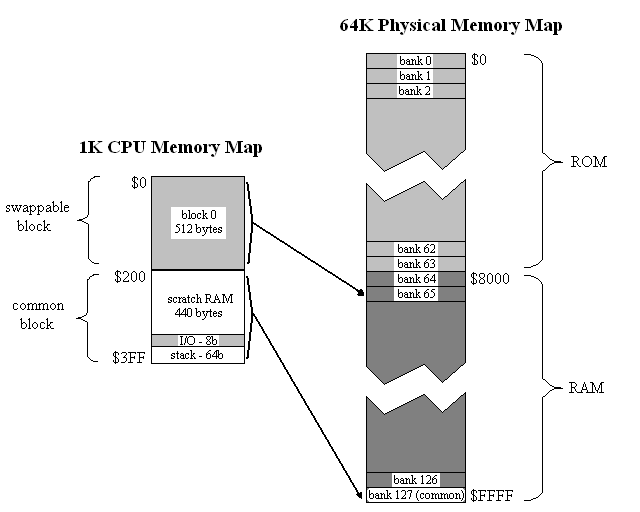
With its 10-bit address bus, the CPU sees 1K of memory. This is divided into two 512-byte blocks. Block 1 contains the stack, I/O ports, and a scratch RAM area. It is the “common” block, and is always present in the CPU’s address space no matter what is happening with bank switching. In contrast, block 0 is a swappable memory area, and can be mapped to any bank in physical memory.
Physical memory is 64K, and is divided equally between ROM and RAM. The 64K physical memory space is partitioned into 128 banks of 512 bytes each. Any bank can be mapped into block 0. Bank 127 is always mapped into block 1, the common block.
The bank select register is part of the memory-mapped I/O ports in common memory. To swap a bank, the CPU only needs to write the new bank number to the appropriate address.
This may all seem pretty simple, but take a minute to consider some of the implications:
- Upon reset, bank 0 is mapped to block 0. That puts 512 bytes of ROM, 440 bytes of RAM, the I/O ports, and the stack all in the CPU’s address space. That’s plenty for many small programs, and means they won’t have to bother about bank switching at all.
- Larger programs (lots of program code) can be accommodated by bank switching code segments in/out of block 0, all operating on common data in block 1.
- Programs operating on large data structures can copy some bank-switching helper code to block 1, then swap additional RAM banks in/out of block 0.
- Arguments can be passed on the stack to ROM helper routines in other banks, because the stack is in common memory.
- All of ROM is addressable, with no holes. This makes storing images, audio samples, and other data in ROM much easier.
- There is no difference in handling between ROM and RAM banks. A program running entirely from RAM works just like one whose code is in ROM.
Failures
While this design seems relatively straightforward, it took me a painfully long time to arrive at it. I went through several days of failed designs before settling on this one.
My first attempt was to divide the 1K space into a 768 byte ROM region and a 256 byte RAM region, reasoning that most programs would have more code than data, and then simply tack the bank select register onto the existing address bus. So A0-A9 came from the CPU, and A10-A17 came from the register. That worked poorly, because it swapped the entire address space at once. With that scheme, there’s no easy way to grow the program code space while sharing the same data, or vice-versa. It also left holes of inaccessible memory within each 1K physical memory bank, and caused the stack to disappear when switching banks. With more tricks some of those shortcomings could be addressed, but it didn’t seem promising.
My second attempt extended the first by disconnecting some of the higher-order RAM address lines. This caused the entirety of RAM to appear several times in the physical address space, at the cost of having less total RAM available. So for example, RAM might be repeated eight times in the physical address space, so that in the 768/256 ROM/RAM partitioning for banks N and N+8, the RAM portion would be the same in the two banks while the ROM portion differed. That provided a way to handle larger programs with lots of code sharing the same data, but not programs working on large sets of data. It also still had the same problems with memory holes. And with the different sizes and fixed locations of the ROM and RAM regions, it would be difficult to bootload a program and run it from RAM in the same way it would normally run from ROM.
I think there was a third, fourth, and fifth idea too, but the details all sort of blur together. They mapped 1K chunks of physical memory into the 1K CPU address space in different ways, combined with a split of the 1K CPU address space into ROM and RAM regions. They all sucked. I went through a lot of pieces of paper.
Eventually I hit on the idea of tying the ROM/RAM select to the bank register, rather than the CPU address. I don’t know why it took me so long to think of that, when it seems obvious now. I devised a scheme with two blocks with a 768/256 split, where either block could be mapped to any 1K bank of physical memory. When mapping a bank to the 768-byte block 0, the upper 256 bytes were inaccessible. And when mapping a bank to the 256-byte block 1, the lower 768 bytes were inaccessible. Yet any byte in a bank was accessible as long as you mapped it to the appropriate block. This wasn’t TOO bad, but was certainly awkward, and it also required two different bank select registers (one for each block).
Finally I went for a long run in the hills near my home. I find that when I’m sitting at my desk, trying to find the solution to something difficult, it never comes. All my good ideas come to me either when I’m driving, in the shower, or out for a run. About three miles in to the run, I thought about a 512/512 split, and realized that if the banks were also 512 bytes, I could fit a whole bank into a block, and eliminate all this weirdness. As I said, it seems obvious now.
There’s one slightly unintuitive aspect to this scheme, which is a result of having 512-byte banks but a 1024-byte address space. The CPU address bus is A0-A9, but A9 is actually not connected to the memory at all! That took me a while to grasp. Instead, A9 is used as a select input to the address decoding logic, and determines whether a memory reference is to block 0 or block 1. It operates the mux that selects either the contents of the bank select register or a fixed value for the upper address lines. The A9 that is actually connected to the memory chips is generated by the decoding logic and is not the CPU’s A9.
Read 3 comments and join the conversation2D Graphics Thingy?
Maybe 3D Graphics Thingy isn’t dead after all. One of my goals for the creation of Tiny CPU was to get more comfortable with programmable logic design, and custom circuit board development, and I’ve certainly done that. Once Tiny CPU is done, I think I’m going to revisit graphics in the form of “2D Graphics Thingy”. My plan would be to work through the memory interface problems that stumped me the first time, and create something like a programmable 2D blitter for a VGA frame buffer. That seems like a manageable project I could expect to succeed at, while also being a step along the way toward the ultimate goal of 3DGT.
Read 5 comments and join the conversation