

Too Many Pins!
The primary components for Plus Too will be the 68000 CPU, RAM, ROM, maybe a microcontroller, and an FPGA containing all the simulated hardware and glue logic. For the FPGA, I’ve been doing some rough estimation of the number of I/O pins and logic resources needed, and it’s a lot! The I/O count looks like it will be at least 117 pins, and that doesn’t even include any allowance for FPGA to microcontroller communication. Because so many of an FPGA’s pins are consumed by power connections and other fixed-purpose stuff, to get 117 user I/Os it looks like I’ll need a device with at least 208 physical pins. Ugh. I’m definitely not comfortable with the idea of soldering that. The 100-pin TQFP in Tiny CPU was bad enough.
Here’s a quick breakdown of how to get to 117 pins:
- 40 – for the CPU address and data bus
- 14 – for other CPU connections like the address strobes, interrupt lines, function code, /DTACK
- 22 – for the address output of the video circuitry (could possibly be reduced to 15)
- 16 – for the parallel load input of the video shift register
- 7 – various select, enable, and output signals
- 4 – keyboard and mouse connections
- 4 – configuration of simulated RAM and ROM size
- 3 – video hsync, vsync, and data
- 5 – other
As I type this, I can already think of a few other signals I forgot, and I’m almost certainly going to need a wide connection between the FPGA and microcontroller too. The final number of I/Os could be in the 140-150 range, forcing me into an even scarier 240-pin QFP package, or the hobbyist’s nightmare BGA package. That’s not good.
While it’s incredibly convenient to lump everything into one giant FPGA that can be reconfigured at will, the huge number of I/Os may force me to split out some functional units separately. The work could be divided across two or more smaller FPGAs, or a single FPGA plus a few well-chosen ICs like bus drivers that need lots of pins but little internal logic. Splitting things up may not be easy, though. In a lot of cases, I’d just end up with two ICs that needed an I/O connection to a signal instead of one, making matters even worse. Only where two wholly unrelated functional modules share the same FPGA could they be split without causing a lot of signal duplication. Splitting things up into more ICs will also result in a larger board, and a bigger PCB routing challenge. I’m definitely beginning to appreciate the difference between a design for a little 8-bit system like Tiny CPU vs a system with multiple 24-bit address and 16-bit data busses.
EDIT: It also looks as if all the candidate FPGAs require a 1.2V supply. Given that I already need 3.3V and 5V for other components in the system, that means I’ll need a three-voltage design. Yuck, yuck, yuck.
Read 7 comments and join the conversation7 Comments so far
Leave a reply. For customer support issues, please use the Customer Support link instead of writing comments.
If you just need more pins rather than more logic, it’s also often cheaper to split the design between several smaller FPGAs rather than one big one. In this case, I suggest splitting the design into 2 FPGAs: one for the control/address busses and the other for the data busses.
The control/address bus FPGA would 1) generate chip selects based on the CPU address, 2) manage the video signal timing, 3) generate the addresses for the video, 4) generate the addresses for the sound data, 5) mux all these addresses (CPU, video, or sound) to the RAM.
The data bus FPGA would 1) load data from the RAM and shift it out for the video, 2) load data from the RAM to control the sound PWM, 3) buffer the CPU’s data bus to the RAM, 4) implement the other peripherals (VIA, RTC) or their emulation (keyboard, mouse).
There would still be a few connections between the two (e.g. chip selects). My main point is that you shouldn’t assume that one high level function (video is the big one here) needs to be entirely in one FPGA or another; it can be split up based on what the subfunctions need to connect to.
Power supply blues: last year I built a digital camera board. Took 5 V in and used switching regulators to generate 3.3 V (microprocessor, SDRAM, and FPGA) and 1.2 V (FPGA). From the 3.3 V I used linear LDO regulators to generate 2.5 V (FPGA) and 2.8 V (CMOS imager chip). Trying to route all those power and ground connections with paths as fat/direct as possible was… interesting.
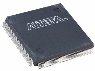
What type of FPGA did you use? I just discovered that all Altera FPGAs from the Cyclone III family or newer have a ground pad on the bottom of the QFP package, which means it can’t be hand-soldered without resorting to the “toaster method”. That limits me to the older Cyclone II family, basically either the EP2C5 or EP2C8. I prefer to stay with an Altera part, since I find the Xilinx documentation baffling and even a Chinese clone of their programming cable is $60.
I know you would probably like to manufacture the whole board yourself, but could you use something like this coupled to a CPU board you make yourself?
(Just a random board I found on ebay that looks like it exposes a lot of I/O)
http://www.ebay.co.uk/itm/Cyclone-III-EP3C10-FPGA-Development-Core-Board-/220599616062?pt=LH_DefaultDomain_3&hash=item335cc3023e#ht_2006wt_1139
I am thinking to learn a bit and start with FPGAs but not able to decide which one to choose from Altera and Xilinx, any suggestions which is going to be best for a starter considering prototype is going to be hand soldered.
After more consideration, I’ve decided to make the initial prototype using a commercially-made FPGA experimenter board, instead of building the hardware myself. It will be more expensive and possibly less fun, but will let me concentrate on whether my logical design is correct without wondering if bugs I encounter are actually caused by hardware problems or soldering mistakes. So I’ll be using a commercial FPGA board with some kind of custom daughter card, like John suggests. Then once I get that working, I can design a version 2 that’s all on a single custom-made board.
I already have a Xilinx Spartan-3A starter board, but I kind of want to crush it under the wheels of my car. It’s mostly irrational, but I’ve developed a strong dislike of Xilinx. The Spartan-3A board also only has DDR2 RAM, and requires the use of a serial cable to program the on-board parallel flash. And since I wouldn’t want to use a Xilinx part for the version 2 all-custom board, it doesn’t make much sense to start with one, other than the cost savings.
I think I’m going to purchase an Altera DE1 board. It’s not the cheapest ($150), but it’s got a Cyclone II 2C20, 512KB of SRAM, SD card reader, and basically everything else I would need except the 68000 CPU. For starters, I can even use a 68000 soft-core running inside the FPGA instead of a physical CPU. The only things the DE1 lacks are a way to connect a keyboard and mouse simultaneously, and enough SRAM to simulate a Plus (this will limit me to Mac 512K simulation). The Cyclone II is the same FPGA family I would likely choose when making an all-custom board, so that would make the transition much easier.
Tinycontrols, you might want to begin with one of the simple boards like the one John linked to, or even a CPLD board like this one from Dangerous Prototypes, then connect it to your own prototyping board. If you definitely want to solder it yourself, then look at the lowest-capacity offerings in Xilinx’s Spartan 3E or 3A line, or Altera’s Cyclone II or Cyclone III, since those are the only ones you can get in a non-BGA package.
I was using an XC3S250E (Xilinx Spartan 3E family) in a TQFP-144 package. It can load its configuration data from an SPI flash chip, so I only needed something that could program the SPI flash rather than something that knows Xilinx JTAG. (Not that this really mattered much, since I also have access to Xilinx programming cables at school)
Or what about these? http://www.actel.com/products/pa3/default.aspx I know nothing about them, or if you can get free software etc. But they did seem to be in better packages?