

Archive for September, 2013
Wire Wrapping the Nibbler CPU
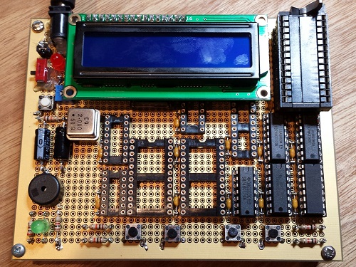
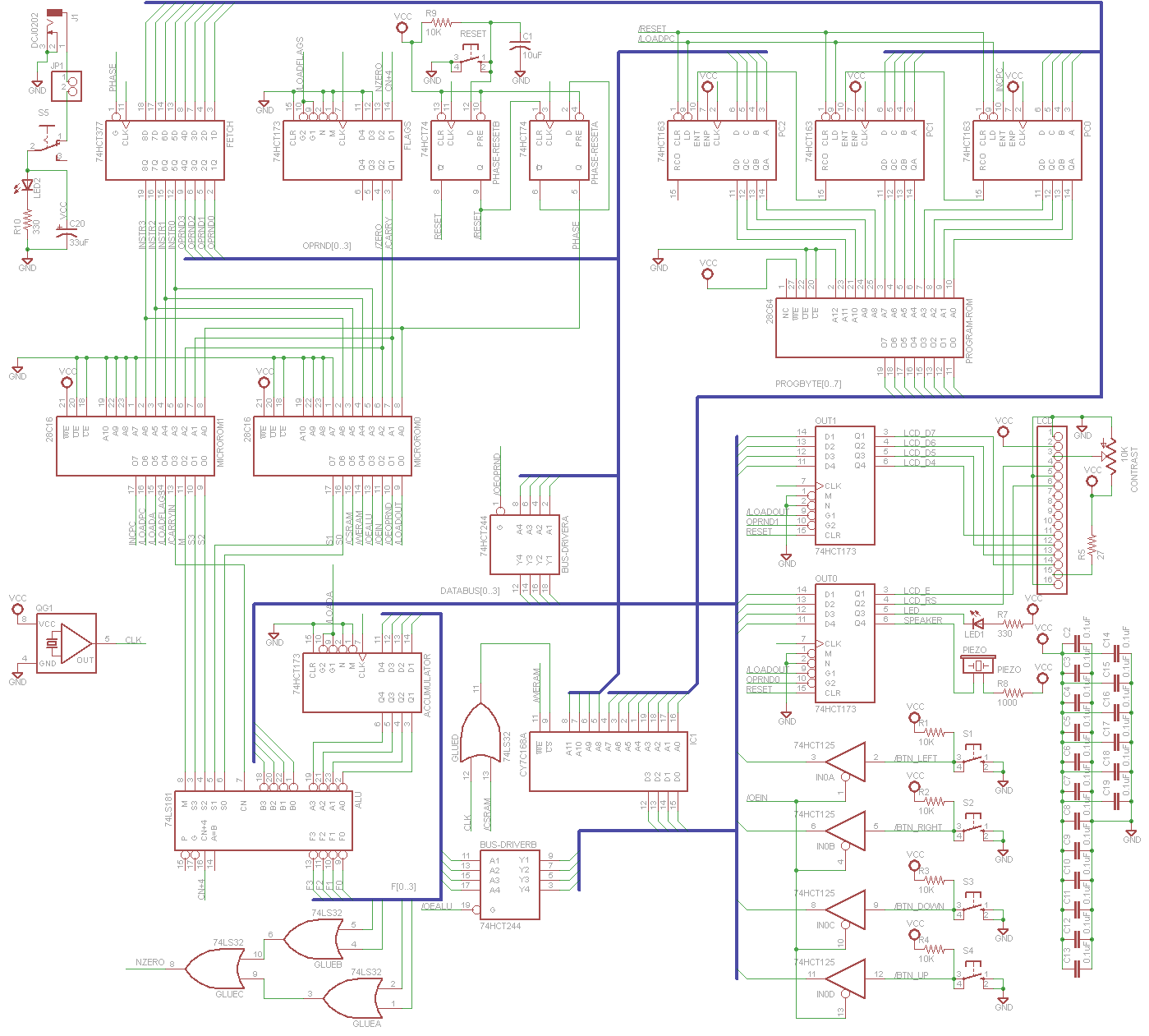
Nibbler construction is underway! I’m building the CPU on a 5 x 4 inch perfboard, and connecting the components using wire wrap. This particular perfboard is a Twin Industries 8200 Series, which has continuous metal planes on both sides that can be used for power and ground. Because the holes don’t go all the way to the edges of the board, the usable area is just 4.5 x 3.5 inches (114 x 89 mm) – about the same size as my mobile phone. It’s very compact. There’s enough extra space for two more 0.3 inch chips, if I later decide to add to the system.
Unfortunately construction didn’t start smoothly. The board didn’t have any mounting holes, and you can see in the photo what a lousy job I did trying to drill four evenly-spaced holes in the corners. After drilling, I made legs by putting screws through the top into 1 inch aluminum standoffs underneath. I quickly discovered that top-side screws in bottom-side standoffs formed an electrical connection, shorting the ground and power planes! Ugh. Inserting nylon washers between the standoffs and the bottom of the board solved that problem, but it wasn’t the last of the challenges.
These kinds of boards are great for mounting and connecting DIP chips, but not so great for anything else like discrete components or buttons. Anything that doesn’t have 0.1 inch spaced pins requires bending or drilling, and discretes also require soldering instead of wire wrap. It took me several hours to drill holes for the DC power jack, deform the button pins to a 0.1 inch spacing, and mount and solder all the other passive components. In many cases that involved cutting a wire so it could be soldered at one end, but wrapped at the other end. What a pain in the butt.
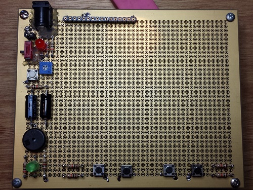
After placement of the discrete components
Soldering anything to this board is surprisingly hard. Each hole is separated from the plane that surrounds it by a circular ring of soldermask. In order to connect a discrete component’s pin to the power or ground planes, the solder must bridge across this ring, and that’s something the solder definitely doesn’t like to do. More and more solder must be added, until it suddenly flows across the ring *and* into the neighboring hole, creating an accidental short. Grrrr! With practice I was able to avoid this, but each solder point was a trial of patience.
After placing all the discrete components, I did a trial fit of all the wire wrap sockets, mounting all the chips inside them. It’s a good thing I did, because there were clearance problems all over the place! If I’d wired up half the system before discovering the clearance issues, I would have been in big trouble. The worst problem was the 74HCT74 for Phase and Reset. Although it’s a 14-pin chip, its package is so elongated, it actually needs more room than other 16-pin chips! I also found a few vertical clearance problems. The LCD is supposed to sit on top of several chips, but I discovered there wasn’t as much space as I’d expected available under the LCD. I’m going to have to build some kind of vertical extension for the LCD, in order to raise it high enough to clear the chips under it.
The last big hurdle was the ZIF socket for the program ROM. I know from past experience that I’ll be swapping that ROM in and out frequently, and I don’t want to have to use a chip puller each time. A ZIF socket will solve the problem, but wire wrap ZIF sockets don’t exist, or are so rare that it amounts to the same thing. I ended up soldering a standard ZIF socket to two rows of machine pin male header, and then inserting the header into a wire wrap socket. It’s not pretty, and the socket sandwich is more than an inch tall, but it works!
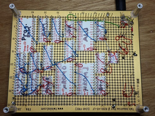
The wiring side, after placement of the power, ground, and clock lines
Son of 3D Graphics Thingy – A Homebrew Graphics Processor

An old project of mine may return from the dead. A few years ago, I started an ambitious project to build a 3D graphics processor using an FPGA. The goal was to create a simple version of the GPU you might find in your PC or video game console – something able to work in tandem with a standard CPU, handling the 3D transform math and pixel rasterization needed to draw pictures of spinning cubes and teapots and things. At the time I was doing a lot of 3D software programming for my job as a game developer, so the idea of building 3D hardware was exciting.
Unfortunately, 3DGT quickly turned into How to Shrink Memory Bandwidth Requirements, How to Build a High Performance DDR2 Memory Controller, and then How to Debug the Xilinx Development Tools, none of which were any fun. I eventually gave up, without ever getting to any of the interesting graphics-related stuff.
Yesterday I happened to re-read my summary of the project, which concluded “Lesson learned: start with a small project and add to it incrementally, instead of beginning with grandiose plans.” That started me thinking about what kind of small and simple graphics system I could build quickly, in order to get something working I could iterate on and improve. Almost all my difficulties with 3DGT were related to DDR2 RAM and the RAM bandwidth requirements, so if I could avoid those problems, I’d be in good shape. The solution seemed simple: use standard SRAM, and shrink the frame buffer size and color bits per pixel, until the memory bandwidth requirements are reduced to an acceptable level.
Specs
For this “Son of 3D Graphics Thingy”, I’m envisioning something like this:
- 512KB of SRAM used for video memory, with a 16-bit wide memory interface
- 20 MHz system clock rate
- 8 bits per pixel, indexed color
- One 640 x 480 frame buffer, or two 546 x 480 frame buffers with double-buffering
- VGA output
- No depth buffer (Z buffer)
- Rasterization only; no 3D transform math
This is a much more modest goal than the original 3D Graphics Thingy. Without a depth buffer or 3D transform support, it’s really more of a 2D triangle rasterizer coprocessor than a 3D GPU. The CPU will be responsible for doing the 3D matrix transformations in software, and drawing objects in back-to-front order to ensure proper depth sorting. It won’t compete with the GeForce, but if I recall correctly, it’s very similar to how the original 1995 Playstation worked.
A 16-bit memory interface running at 20 MHz has a max theoretical throughput of 40 MB/s. So what can we do with that? Let’s assume each pixel is cleared to black at the start of each video frame. Then the pixel is written to four times, by four overlapping triangles (the scene’s depth complexity is 4). Finally the pixel is read by the VGA circuit, to generate the video signal output. That’s 6 memory operations per pixel, at 8 bits per pixel (one byte), so 6 bytes per pixel per frame.
Assuming a 640 x 480 frame buffer, each frame will involve 640 x 480 x 6 = 1.84 MB of memory I/O. Dividing that into the 40 MB/s of available video memory bandwidth results in a top speed of 40 / 1.84 = 22.8 frames per second. With only a single buffer, you’ll see screen tearing while objects are animating, which isn’t ideal, but it works.
Plan B is to use two 546 x 480 buffers, and draw objects into one buffer while the VGA circuit generates a video signal from the other buffer. This rather strange frame buffer size was chosen because two buffers fit exactly into 512 KB. Probably the VGA circuit will add black bars on the left and right of the image, pillar boxing the 546 x 480 image inside a standard 640 x 480 video signal. With a 546 x 480 frame buffer, each frame will involve 546 x 480 x 6 = 1.57 MB of memory I/O, resulting in a top speed of 40 / 1.57 = 26.7 frames per second. 26.7 FPS isn’t exactly speedy, but it’s fast enough to draw animated objects. And thanks to double-buffering, you won’t see any screen tearing.
Building It
Now I need to design a board with a CPU, an FPGA, and some SRAM, right? Actually, no I don’t. The Altera DE1 board that I used for Plus Too already has everything I need. Its FPGA is large enough to implement both a soft-core CPU and the custom graphics core, and it’s got 512 KB of SRAM with a 16-bit wide interface. The SRAM has a 10 ns access time, so better performance than I described above is possible if I can boost the clock speed above 20 MHz. And the board also has 8 MB of SDRAM, if I ever get brave enough to make another attempt at writing a memory controller. It looks like other people already have working examples of SDRAM controllers for the DE1, so maybe it wouldn’t be that bad.
So that’s the plan. I’m not expecting to start building this tomorrow – I still have my Nibbler CPU project to finish, and other projects I’d like to pursue – but it’s an interesting idea. My problem is too many ideas, too little time!
Read 6 comments and join the conversation
Nibbler Refinements
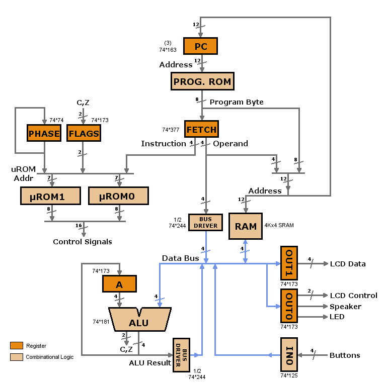
I’ve made a few refinements to the Nibbler design, and now I’m ready to start building the CPU! After looking at what seemed like a million different possible changes and additions, I’ve decided to keep the hardware exactly as I originally described it in my first post, with just a few minor changes:
- Replace the ‘175 quad flip-flop with a ’74 dual flip-flop
- Add a ’32 quad OR chip for glue logic
- Replace the ALU’s Equal flag with a Zero flag
- Replace the 2K x 8 RAM with a 4K x 4 RAM
The addition of the OR chip makes the last two changes possible. And although Nibbler will have one more chip than before, I believe it actually makes the overall design simpler to understand.
Flip-Flop: The ‘175 was used for the /RESET signal, and the Phase bit. Because I was only using two of the four FF’s on the ‘175, switching to the smaller package of the ’74 makes sense. The ’74 also has independent clear inputs for each FF, so now /RESET can force Phase to 0, which wasn’t possible with the ‘175.
Zero vs Equal: The original design had an Equal flag, which was set by the ALU’s A=B output as a result of the CMP instruction. This was OK, but a Zero flag is better. It’s set by any instruction that modifies the accumulator, as well as CMP. That makes it possible to do a LD, IN, or NOR, and follow it immediately with a conditional jump JZ or JNZ, without ever doing a CMP. That wasn’t possible with the Equal flag.
The Zero flag is generated by using three OR gates to OR together the 4 bits of the ALU result: /Zero = (F0+F1)+(F2+F3). I considered an alternative method, where the ALU is operated in active low mode, and the operands and output treat a low voltage as logical 1 and a high voltage as logical 0. This makes the ALU’s A=B output behave like a true Zero flag, but requires the use of some inverting buffers, and requires some staring at the datapath diagram and the datasheet before it’s clear why it works. The OR method is much more intuitive.
4-Bit RAM: My original plan called for an 8-bit RAM, with four of the data pins unused. That’s a little awkward, but because none of the 4-bit RAMs I found had a /OE output enable, they couldn’t be used with Nibbler as-is. 8-bit RAMs typically have a /OE pin, making them easier to work with. The reason is somewhat complicated. With only /CE and R/_W inputs on the 4-bit RAM, it’s not possible to enable it for appropriate instructions and gate the write-enable signal with the clock (necessary to prevent accidental writes) without external glue logic.
With the addition of the ’32 quad OR chip, I can use one OR gate for the necessary glue. The /CERAM control signal is OR’d with the clock, and connected to the RAM’s /CE input. This ensures that RAM is only enabled during the second half of the clock cycle, and only during clock cycles where the microcode wants it enabled. The /WERAM control signal is connected directly to the RAM’s R/_W input. If it’s enabled and it’s not writing, then the RAM functions in read mode, and drives a nibble onto the data bus.
New Instructions
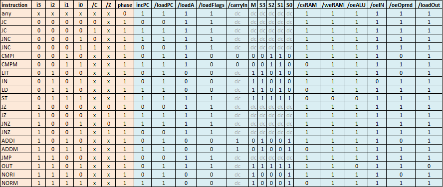
What about possible new instructions? I’ve decided to keep things as simple as possible, and stick to 16 instructions, selected by the high 4 bits of a byte of program memory. Furthermore, I’m only going to consider instructions that can work with the current datapath and control path, and can be implemented solely by changing the microcode ROM contents. That rules out many of the possible new instructions that I discussed previously, but keeps everything much simpler.
So, exactly which 16 instructions will it be? I’m not sure yet, but I don’t have to be. I can update the contents of the microcode ROM after the CPU is built, based on my experience writing programs for it, to select the 16 instructions that prove to be most useful. However, 14 of those 16 are almost certain. The only real question is whether JNZ and JNC should be replaced with something else.
Incidentally, I never realized the double-entendre in “driving the data bus” until now. Maybe when I retire, I’ll buy an old yellow school bus, paint DATA BUS on the sides, and drive it to electronics shows shouting out the window “Look, I’m driving the data bus!” Fun times, guaranteed.
Read 11 comments and join the conversation
Inside Vintage Electronic Toys – How Speak & Spell Works
The 1970s were a great time to be a geeky kid, thanks to the introduction of the first digital electronic toys. With their beeping songs and blinking lights, who could resist them? Recently I decided to take a trip down memory lane, buying some classic 70s digital toys, and carefully disassembling them to reveal their vintage electronic guts. For about $50 and some time spent on eBay, I found myself the proud new owner of a Little Professor calculator, a Mattel Electronic Football handheld game, and the gem of the collection: a Speak & Spell talking toy.
Batteries
Today most portable electronics use a couple of AA or AAA batteries, but not these vintage devices. Little Professor and Football both need a 9V battery, and Speak & Spell actually uses four C cells. C cells?? I don’t think I’ve ever seen those used anywhere except flashlights and things with motors. The designers must have anticipated some major current demands that would have exhausted 9V or AA batteries too quickly.
The popularity of 9V batteries may have been because older semiconductor technologies often required higher voltages, like 9V or higher, compared to today’s chips that run at 5V, 3.3V, or even less. It’s also possible that classic devices relied on linear regulators to bring 9V down to the required 5V, but modern devices typically use boost regulators to bring 1.5V or 3V up to their required voltage.
Display
Another shared feature that caught my attention was the displays. None of the toys has an LCD display, and certainly not an LED display. In the mid-to-late 70s when these toys were made, LCDs were high tech and out of reach for cheap consumer devices. Instead of an LCD, Little Professor and Football both have red matrix LED displays, and Speak & Spell has a blue vacuum-fluorescent display that looks like something out of a sci-fi movie. Very retro!
Little Professor – Texas Instruments (1976)
The oldest of the bunch is Little Professor, first released by Texas Instruments in 1976. Over the years it went through many revisions, with different displays and buttons. The original version is shown here.
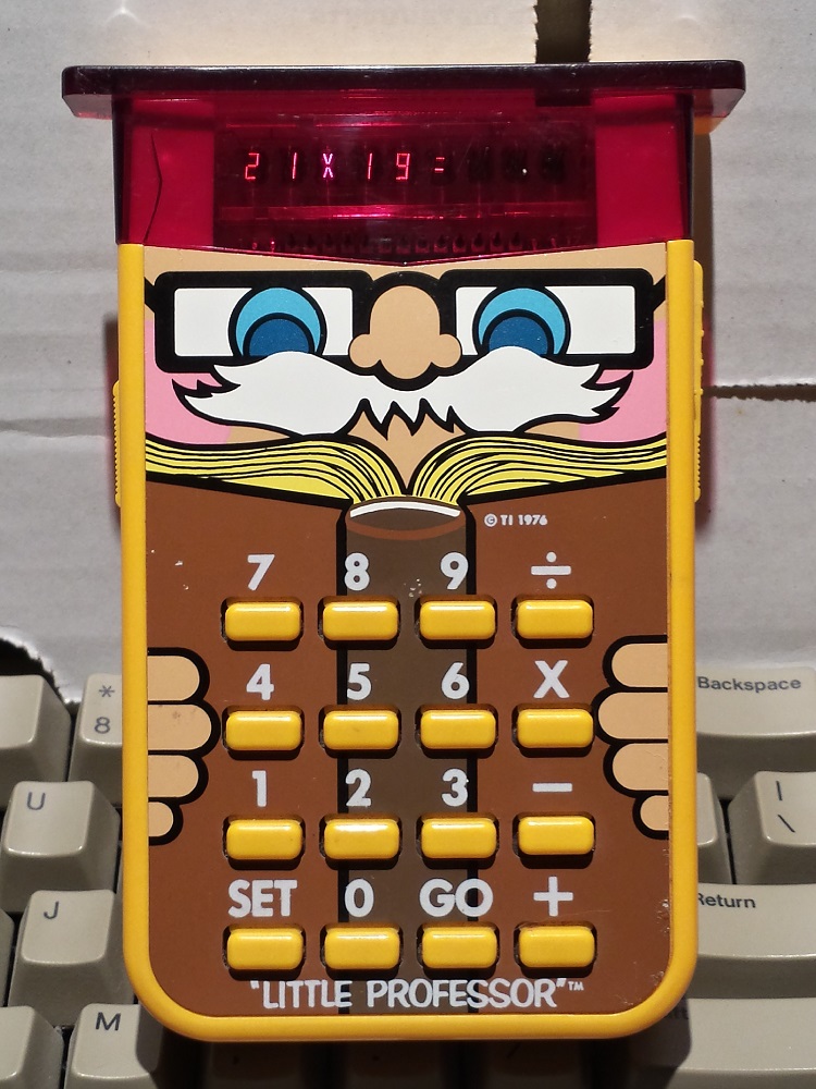
Little Professor is essentially a calculator in reverse: the display presents a math problem, such as 21 x 19, and the player must enter the answer. If the answer is correct, a new math problem is presented. An incorrect answer flashes EEE on the display. There are no sound effects, and no feedback of any kind beyond the numeric display. It’s drill-and-practice at its dullest, yet TI managed to sell over 1 million units in 1977.
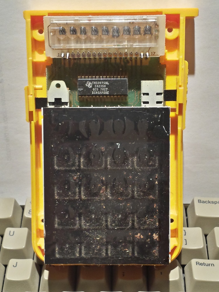
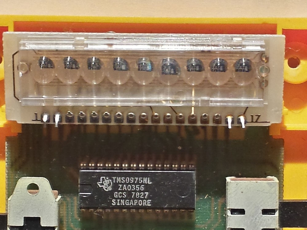
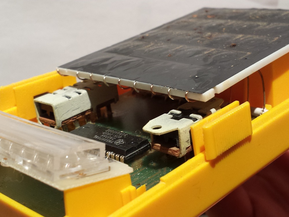
Peeking inside reveals very few parts, and the contents are mostly empty air. There’s a membrane keyboard, LED matrix display, two slide switches for on/off and difficulty selection, and a single 28-pin SDIP (shrunken dip). That’s it. There’s not a single resistor or other passive component anywhere.
The secret to the low part count is that chip: a TMS0975 microcontroller. It’s a member of TI’s TMS1000 family, and a sibling of the TMS0972. These microcontrollers were widely used in other “real” calculators of the same period. They were 4 bit architectures, with three data registers, 1KB of ROM, and 32 bytes of RAM. The nominal clock speed was only 400 kHz. Unlike today’s microcontrollers, the ROM store was not re-writable, so once a program was stored in the MCU it was fixed forever.
Beyond the microcontroller functions, the TMS0975 also incorporated the LED digit drivers, keypad input, clock oscillator, and other elements. No external passive components were required. This would have helped keep manufacturing costs low. TI probably made a nice profit selling these at $20 apiece – that’s $82 in 2013 dollars!
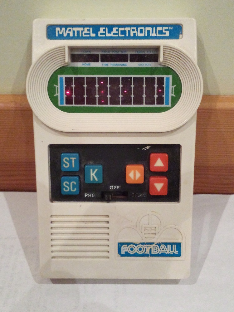
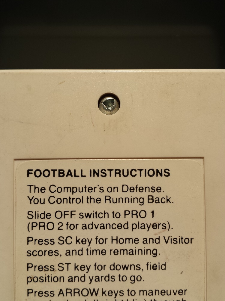
Mattel Electronic Football – Mattel (1977)
Electronic Football was one of the first releases in Mattel’s long-running handheld sports series. And to be clear, we’re talking about American football here, not soccer. Two players take turns running offense, while the computer handles defense. The goal is to maneuver the bright red blip (the running back) through the dark red blips (the defenders) without being tackled.
Bright and dim red blips? It’s hard to imagine how this game could have been successful. Released in the summer of 1977 and sold through Sears, Electronic Football sold poorly at first. Sears used a computer model based on initial sales data to conclude the game wouldn’t be a major seller, and manufacturing was halted after fewer than 100K units were made. Then in mid-January 1978, Sears told Mattel they’d made a mistake, and that they wanted 200K units a week. By mid-February 1978, manufacturing reached the previously unknown level of 500K units per week. 500,000 Electronic Football toys shipped to Sears stores, every week! Wow.
This is Screwy
Getting inside the toy’s case was challenging. It’s held together with three security screws, requiring some kind of triangular screwdriver that doesn’t seem to exist anywhere, even in specialized bit sets. Really Mattel? Why? Their game was rather famously cloned by Coleco as “Electronic Quarterback”, so maybe this was Mattel’s attempt at preventing people from peeking under the covers and stealing the design, but it’s hard to imagine how security screws would have prevented corporate IP theft.
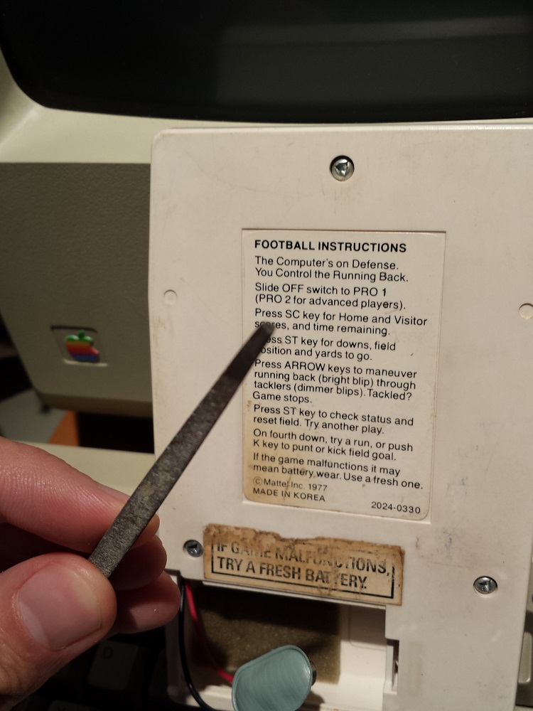
I searched the web to see if anyone else had a solution for the triangular screws. One person claimed they could be removed with a flat blade screwdriver, inserted just so, but nobody else was able to duplicate this feat. Certainly it didn’t work for me. Other discussions centered on making a custom screwdriver blade. In desperation I went rummaging through my toolbox, and discovered a three-sided file whose pointed end was exactly the right shape and size to fit the screws. Hooray!
Mattel’s Secrets Revealed
Once opened, the Electronic Football case revealed a single low-density board with the Rockwell International logo, and an attached speaker. By carefully removing the board and turning it over, I exposed Mattel’s hidden secrets. As with the Little Professor, there were surprisingly few components inside: just a membrane keyboard, an LED display, a slide switch, a resistor and a capacitor, and one mystery chip. The LED display was an interesting affair, with a calculator-style 7 segment display matrix in one half, and a 9 x 3 LED “football field” in the other.
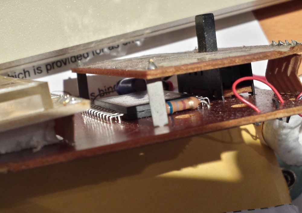
Unfortunately the mystery chip was obscured by the keyboard, which was soldered in place, and I didn’t want to do anything destructive to gain better access to it. According to information I later found on the web, it’s a Rockwell B6100-15, which is a modified calculator chip not unlike the brains of the Little Professor. Further details were revealed in this interview with Mark Lesser, the Rockwell engineer who designed the circuitry and wrote the software for Electronic Football. Development was challenging, as the chip only had 512 bytes of program memory, and the assembler ran on a mainframe computer at Rockwell. The program was entered as a batch job using IBM computer punch cards.
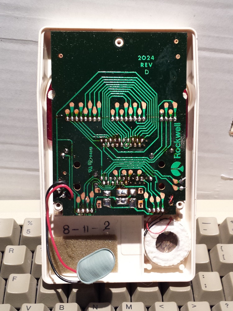
I never found a satisfactory explanation for how the playfield blips were switched between dim and high brightness, providing three possible states for each blip: off, dim, or bright. This implies a changing voltage across the LED, but the LEDs were driven directly by the Rockwell chip, which presumably had digital outputs with only two states.
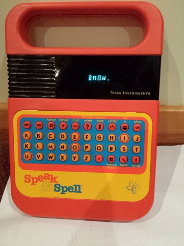
Speak & Spell – Texas Instruments (1978)
Texas Instruments released Speak & Spell in 1978. Looking back on it 35 years later, it’s hard now to appreciate just what a huge sensation it was. It talked! While today every phone and camera seems to have voice features, in 1978 this was unheard of. Some earlier toys like Chatty Cathy managed a few phrases of pre-recorded speech stored on tape or miniature phonograph discs, but nothing matched the verbosity or sophistication of Speak & Spell.
When E.T. used a Speak & Spell to phone home in 1982 (along with an umbrella, a circular saw, and some other junk), its lasting popularity was ensured. It became an international success, released as La Dictée Magique in France, Grillo Parlante in Spain and Latin America, and Buddy in Germany. Speak & Spell eventually went through many revisions, switching to an LCD display and a different keyboard, among other changes. The original 1978 version with blue vacuum fluorescent display is shown here.
The premise of Speak & Spell was simple. A synthesized voice would prompt the player for something like “spell ocean”. After dutifully typing O-C-E-A-N, the player would hear “that is correct”, followed by another word. A mistake would result in hearing “wrong” or “that is incorrect”. There were just enough alternative phrasings for correct/incorrect words to keep it from becoming repetitive, and the total spelling vocabulary was about 200 words. Expansion modules placed in the battery compartment could add a new vocabulary of an additional 200 words.
Under the Hood
As expected, the guts of Speak & Spell proved to be substantially more complex than either Little Professor or Electronic Football. After removing the back cover, I found a medium-size board connected to a speaker, with an expansion module attached. Hidden underneath were two membrane keyboards, one for each half of the button array on the front panel.
Removing the circuit board was more difficult than it first appeared. It was attached to the keyboards with stiff copper wires, and the keyboards were held on the front cover by plastic clips. Gentle prying on the plastic clips failed to release the keyboards, and more robust prying broke off two of the clips. $@&*#! After a lot of patient poking and wiggling and bending, I was finally able to remove the circuit board and keyboards, and flip them over to reveal the heart of the beast.
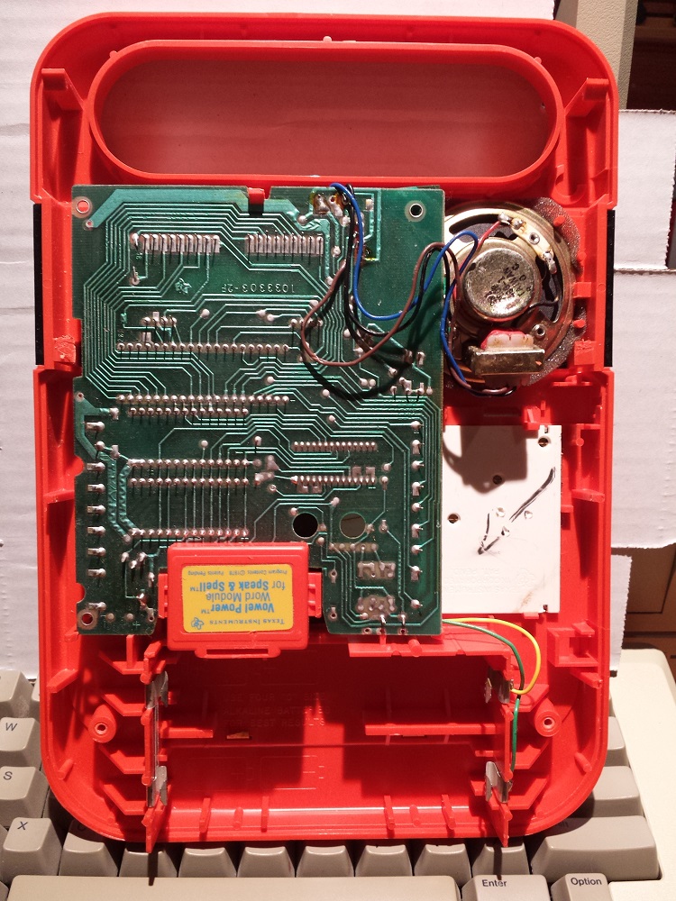
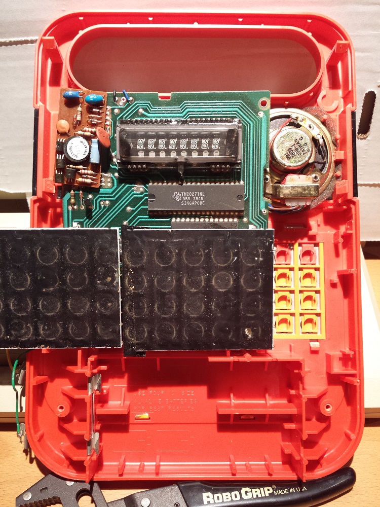
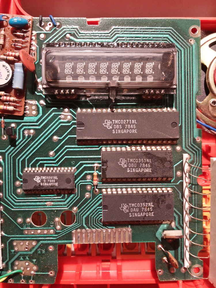
The brown board at top-left of the photo is the power board. It turned out to be a miniature switch-mode power supply, tucked inside the Speak & Spell! The rest of the goodies are on the green logic board, including the eight-character VFD display, and four custom TI chips. This is where all the magic happened.
Closest to the display is the 40 pin TMC0271 microcontroller, another member of the TMS1000 family. This 4 bit MCU had 2KB of program ROM, and 128 nibbles of RAM. Each instruction took six clock cycles to execute, at nominal clock speed of 320 kHz, for total throughput of 0.05 MIPS. It wasn’t blazing speed, but it got the job done.
At left and below the MCU is the 28 pin TMC0281, which was TI’s new single-chip voice synthesizer. More about this in a minute.
Below the MCU to the right, there are two ROM chips labeled TMC0351 and TMC0352. These 16KB ROMs were the largest available at the time, and were used to store speech data. Another 16KB ROM was discovered inside the expansion module when I cracked it open – this one labeled TMC0350. These ROMs didn’t have standard parallel or serial interfaces, but were strange designs containing an address counter and control circuitry in addition to the memory. By tracing the circuit board, other hackers have learned that the ROMs don’t interface to the microcontroller at all, but are driven directly by the speech synthesizer. Maybe that explains their strangeness.
Making it Talk
So how did Speak & Spell create human-sounding speech? It represented words as a series of phonemes, each one 25 milliseconds long. Each phoneme was generated by seeding the voice synthesizer with appropriate data. The synthesizer contained two audio oscillators. A periodic “chirp” oscillator produced a sound like a man saying “uhhhhh”, and was used to create voiced phonemes like the letter “O”. A separate noise oscillator was used to create unvoiced phonemes, like the letters “T” or “S”.
By controlling the volume and pitch of the oscillators, and further tuning their sounds by using a 10th order digital filter, a wide variety of speech-like sounds were possible. Encoded speech was very compact, requiring at most 12 numbers per phoneme: volume, pitch, and the 10 filter coefficients. By using repeat flags and omitting filter coefficients in some circumstances, the data was reduced still further. The average bitrate of speech encoded this way was about 1000 bps (125 bytes/sec). Thus the 16KB ROMs each provided space for about two minutes of encoded speech. Many more details on the synthesizer and the encoding mechanism can be found at furrtek.org.
In theory, it was possible to create synthetic speech by sitting in a quiet room and authoring synthesizer coefficients by hand until the desired sound was achieved, but this approach was incredibly time-consuming. Instead, Texas Instruments used a mainframe computer to analyze recordings of real human speech, and map them to the closest synthetic phoneme for each 25 ms interval. A radio DJ from the Dallas area was chosen as “the voice of Speak & Spell”, because his monotone delivery and deep voice could be efficiently encoded.
Speak & Spell was a fascinating product, with many more interesting details than I’ve described here. For more, check out this great technical article by one of Speak & Spell’s original designers at cnx.org.
Read 3 comments and join the conversation
Guess the Number
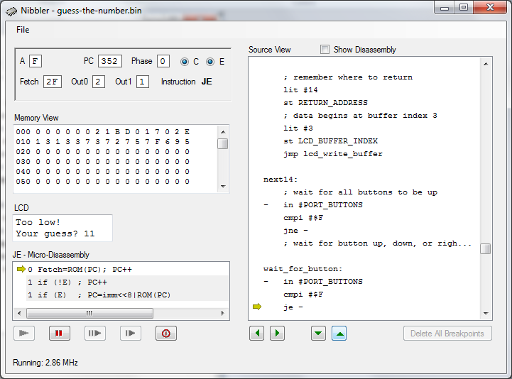
It’s programming time! To verify that Nibbler’s design and instruction set are powerful enough to handle a real program, I sat down to write a simple “guess the number” game. And… (drumroll) it works! I ran the program on the Nibbler simulator, and interacted with it using the simulated pushbuttons. Hint for competitive players: you can always guess the number in at most log2(range) guesses. 🙂
At startup, the program asks the player to press any button. While it waits, it constantly increments a 4-bit counter, incrementing from 0 to 15 and rolling over back to 0. The value of the counter when the player presses the first button determines the secret number he’ll be trying to guess.
Next, the program prompts the player to enter a guess. Pressing the up/down buttons increases/decreases the guess number, and pressing the right button submits the guess. The guess number is converted to text using a crude nibble-to-ASCII conversion routine, which does a byte-wide addition of the number to the character literal ‘0’, performing carry propagation from the low to the high nibble. After submitting a guess, the LCD display changes to “Too high!”, “Too low!”, or “You got it!”, and the player is prompted for a new guess. View the Guess the Number program listing.
While the program runs perfectly on the simulator, there are a few details that probably need to change to make it work on real hardware. Button debouncing code needs to be added, since real buttons don’t cleanly change between their 0 and 1 states, but bounce rapidly between states for a few milliseconds when the button is pressed or released. The LCD initialization and timing code may also be off – I’ll need to verify that on real hardware to be sure.
Program Analysis
The guess the number program assembles to 1135 bytes, or 27% of Nibbler’s program memory. Writing the program was an interesting exercise in coping with the limitations of the CPU’s simple design:
- Registers – Nibbler has just one CPU register: the 4 bit accumulator “A”. Surprisingly, working with only one register didn’t cause many problems, and there were few instances where additional registers would have made a difference.
- Call/Return – The lack of a stack in Nibbler means there’s no call/return mechanism, so no way to call subroutines in the traditional way. This was an annoyance, but I was able to work around it by using a dedicated memory location called
RETURN_ADDRESS, and testing its value at the end of subroutines in order to determine where to jump next.
- Indirect Addressing – All Nibbler memory references use absolute addressing, with no indirect or indexed address modes. This was a bigger annoyance, and working around it led to some ugly code bloat. To get the Nth element from an array of size K, the code must perform K tests of the value of N to determine the correct absolute address. This approach would be impractical in a system using large data structures, but for the types of programs planned for Nibbler, it works OK.
- Program Literals – The biggest headache turned out to be working with arrays of constant data: the character strings like “Press any button”. These had to be copied to data memory one nibble at a time, using LIT and ST instructions, resulting in major code bloat. With this technique, each nibble of constant data requires three bytes of program space. With 4096 bytes of total space, this limits Nibbler programs to a few hundred bytes of strings and other constant data, but that should be enough.
Tool Updates
Along the way, I made a few improvements to the toolchain. The Nibbler assembler gained the ability to do basic math on address labels, such as
ld LCD_BUFFER+1
to load the accumulator from the second nibble of LCD_BUFFER. This proved to be extremely useful, as you can see in the program listing.
The second major improvement was to the simulator. I grew curious how fast the simulation was running in comparison to the planned clock speed of the real hardware, so I added a simulated MHz status line at the bottom of the simulator window. It turns out that the simulation runs faster than the real thing, averaging about 3 MHz when running on a 2.5 GHz Core i5 computer. Not bad for managed .NET code that was written with no thoughts for performance optimization.
Read 17 comments and join the conversation