Archive for June, 2016
Dirty PCBs Review
Today’s electronics hobbyists are blessed with many options for custom PCB manufacturing, like Seeed, Elecrow, and OSH Park. For around $1 to $2 per board, depending on size and quantity, these vendors will turn your EAGLE or KiCad or other Gerber files into shiny new PCBs. I’ve used all three in the past, but my go-to vendor for most things is Seeed.
Dirty PCBs is a newer entry in this space, but it’s affiliated with Dangerous Prototypes, who are long-time members of the hobbyist electronics community. A few years ago Ian Lesnet moved himself and the company to Shenzhen, China, and Dirty PCBs is sort of a matchmaking service between Shenzhen PCB manufacturers and hackers around the world. For a recent PCB purchase of 20 boards, I decided to give them a try.
Saving Pennies
The main attraction of Dirty PCBs is the price. Even among other cut-rate PCB manufacturers, it stands out as the cut-ratest. Any color PCB is available for the same cost, whereas most manufacturers charge extra for colors other than green. Slow-boat shipping is free worldwide, and the faster shipping options tend to be cheaper than at the competition. For my order of 20 red PCBs, 10×10 cm size, shipped by DHL China, here’s how Dirty PCBs compared to Seeed:
10×10 cm PCB @ qty 20 = $57.43
Red soldermask = $10.00
DHL shipping to USA = $24.71
TOTAL = $92.14
Dirty PCBs
10×10 cm PCB @ qty 20 = $50.00
Red soldermask = $0.00
DHL shipping to USA = $15.00
TOTAL = $65.00
Dirty PCBs also uses a constant price per board as you increase the quantity, or offers a small discount for larger quantities, as you would typically expect. Seeed has the bizarre habit of offering a negative “discount” for higher quantities. E.g. with Seeed it’s sometimes cheaper to buy 10 boards twice than to buy 20 boards.
Ordering
My biggest gripe with Dirty PCBs is the website itself and the way it’s marketed. The site’s tagline says “No bull, just crappy PCBs.” I suspect I’m in the minority, but I just don’t appreciate the joke here. Call it basic, no-frills, or rock-bottom if you like, but please don’t tell me I’m paying money for something that’s intentionally crappy. Especially when, if you read the specs and the terms, it’s not crappy at all. Yet I’m somehow left with a mental picture of a sloppy, careless, and all-around half-assed manufacturing process. I don’t think it’s accurate, but that’s the image it paints in my mind.
To be fair this attitude is intentional, and can be traced to the “accidental” launch of the Dirty PCBs service. As Ian tells it, he never meant to launch a PCB service, but simply hacked together some scripts for the convenience of his friends. That unofficial “for friends” service became unexpectedly popular, and Dirty PCBs was born. Ian’s said in the past that the service doesn’t really make any profit, so his tolerance for whiners and time-wasters is low. To quote the About page:
This site was intended for friends and not the public. We’ll process your boards, but we only make about 30 cents per order. We really don’t care if you want to take your business somewhere else, and it’s not worth our time to deal with stupid questions or asshats. Paypal fee reversals, annoying emails and the like will get you banned from the site.
Fair enough, and +1 for use of the word “flippant”. The actual ordering process was simple, except for a mistake I made when uploading the Gerber files. The upload button doesn’t mention what file format it expected (I later found this information on the About page), so I uploaded a zip archive of the same Gerbers I would normally send to Seeed. It appeared to work, and I went through the entire checkout and payment process, only to be informed after I’d paid that no board outline file was found. This was because my Gerbers had different filename extensions than Dirty PCBs was expecting. After renaming the files and uploading a new zip archive, all was well.
Delivery
My order was placed on Thursday afternoon, and the finished PCBs were in my mailbox on the following Wednesday afternoon. Six days! That is crazy fast. Maybe I just got lucky and hit the manufacturing cycle at the perfect time, but that’s more than twice as fast as any other PCB order I’ve ever made in China or the USA.
Inside the box was an unexpected surprise – 23 PCBs instead of 20. I know the Dirty PCB’s proto-pack is “about 10” and often 11 or 12, but I didn’t realize they did a similar thing for larger orders. Presumably they make 10% extra in case some PCBs fail the e-test, then mail you all the boards that passed testing. So hey, three extra free boards. Thanks!
Inspecting the Boards
Now for the key question: were the boards any good? From my inspection, I’d say mostly yes. I spent a long time examining the boards under 10x magnification, and comparing them to my original EAGLE files, and to the Gerbers using gerbv. Probably I’ve never examined any PCB quite so intensely, and some of the issues mentioned below may be typical of other discount PCB manufacturers too. For the money paid, I’m not complaining, but for completeness I’ve catalogued the good and the not-so-good.
The Good
First and foremost, my sample PCB worked great once I populated the components and put everything together. This is about the only thing that really matters in the big view, and it means there were no accidental shorts or breaks in the PCB traces. Of course I hadn’t really expected any problems there, since Dirty PCBs advertises a minimum 5 mil trace/space size, but I only went down to 8 mil and was nowhere near the limit.
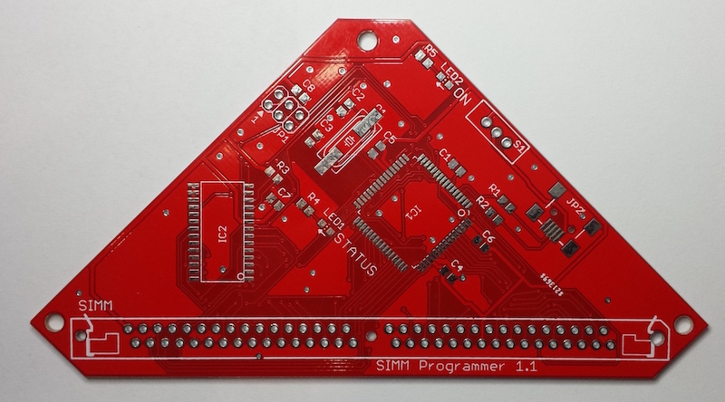
My board is a rather funky hexagon shape, or a triangle with clipped corners if you prefer. There were no problems routing this non-standard board outline.
When examined under magnification, all the drill holes appeared nicely centered in the vias and pads. The edges of traces and planes appeared clean and crisp. Silkscreen was sharp and nicely legible. The soldermask was a nice bright red color, and tented vias were actually tented.
The Not-So-Good
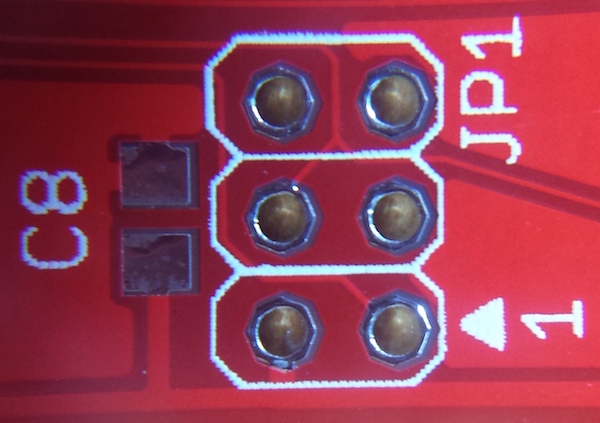
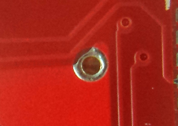
One small gripe: the silkscreen layer was slightly offset from the copper layers and drill holes, as you can see in the photo below. The silkscreen outline for this AVR ISP footprint isn’t centered around the pads. This doesn’t matter much, but it may bother you if you’re a stickler for little details.
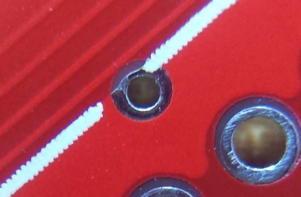
One bigger gripe, that I’m still not sure is my fault or Dirty PCBs’ fault: some of the extra-large vias appear either larger than intended, or not in the right place – it’s hard to be sure which. Here’s an example of a large untented via that connects ground planes on the top and bottom of the board. In the photo, notice how the edge of the drill hole is almost exactly in line with the edge of the ground plane (which is partly obscured by the silkscreen line)? And the plating around the drill hole actually extends beyond the ground plane, bowing outwards slightly into the gap between the ground plane and the neighboring trace? And the stop area (the area without soldermask) extends nearly all the way to that neighboring trace?
Here’s the same region viewed in EAGLE, with the silkscreen hidden. Notice that the drill hole comes well short of the ground plane’s edge, the plating around the hole doesn’t extend beyond the edge, and the stop area only extends maybe one-third of the way into the gap between the ground plane and the neighboring trace.
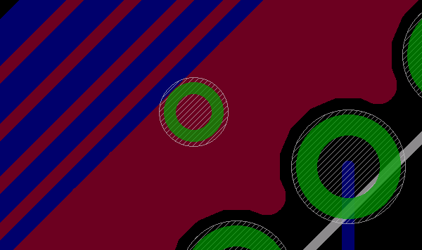
And here’s the same region once more, looking at the actual Gerber files with gerbv. The top copper layer is magenta, drill holes are lavender, and the stop mask is gray. Maybe the Easter Bunny chose this color scheme. Where layers overlap you’ll see additive coloring. There’s no separate color for the plating around the hole here, since both the plating and the ground plane are just part of the top copper layer. It almost looks like Dirty PCBs interpreted the stop mask layer (gerber.GTS) as an additional top copper layer, than generated its own stop mask around that.
Another possibility jumps to mind as I type this: I used a non-standard drill size for those extra-large vias of 0.02362205 inches – not sure how that happened. I wonder if DirtyPCBs rounded up to the next larger drill size, then automatically enlarged the copper area and stop mask to compensate. The through-hole pads in these pictures use a 0.040 inch drill, so the ratio of the hole sizes should be 0.02362205 / 0.040 = about 0.59. But measuring the actual hole size ratio observed in the PCB photo, it’s about 0.62. So those via holes are about 4.7% larger than they were intended to be, if my figuring is correct.

Here’s another example of the same issue. This via bulges outward slightly from the top-left of the ground plane, and the stop area extends all the way to the neighboring trace. But in the source file, the via’s drill hole and plated area are both completely within the boundaries of the ground plane, and the stop area only extends about a quarter of the way to the neighboring trace.
Overall Rating
As an overall rating, I’m giving Dirty PCBs a thumbs-up. They were cheap, super fast, sent me extra boards, and the boards worked. I’m not sure I’d trust them yet with a design that goes all the way to the 5 mil limit, but it’s probably best to avoid that limit anyway. I wish they’d change the name or at least the tagline, but that’s just me. I expect I’ll use Dirty PCBs again, and will report how it goes. Thanks for reading!
Read 6 comments and join the conversationDiscovery Day!
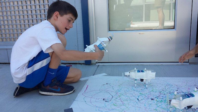
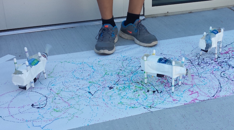
Every year I lead a group of kids in the construction of an “Electric Scribbling Machine”, as part of the local elementary school’s Discovery Day program. The program sessions are run by parents and local community members, and can be anything from karate to marshmallow cannons to frog dissection. The kids range in age from 7 to 10 years, and the sessions are only 50 minutes long, so it’s a challenge to design interesting projects to fit the available time and skill level of the kids. Despite the challenges, we always manage to have lots of fun!
The scribbling machine concept is simple:
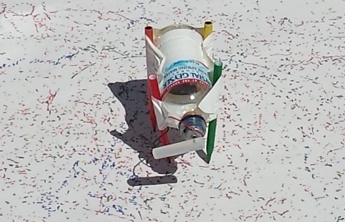
- Attach an off-center weight to an electric motor, so it wobbles and vibrates
- Attach the motor to some kind of body
- Attach colored markers to the body as “legs”
- Set the machine on a large sheet of paper, and watch it go!
I use cheap DC hobby motors rated for 1.5V to 6.0V, with an AA battery. The off-center weight is a glue stick (designed for a hot glue gun), with a small pre-cut hole that press-fits onto the motor shaft. The body is an empty plastic water bottle, and the legs are washable Crayola markers. What could go wrong?
If you guessed there would be tons of problems, you’re right. In past years, we used rubber bands to hold the battery and legs to the body, and the motor wires to the battery. Kids and rubber bands don’t mix well in this project – most of them lack the physical dexterity needed to twist a rubber band around two objects and hold them in place. They struggle with it, accidentally crush the water bottle, and get frustrated. Rubber bands on the battery for the motor wires are also a problem. You can imagine how unreliable that connection can be, and there’s no easy on/off switch.
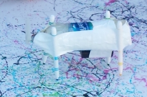
A New Design for 2016
This year we made two big changes to the design. I bought a pile of 2xAA battery holders with an integrated on/off switch, for a much simpler and frustration-free electrical connection. And I replaced all the rubber bands with duct tape. Who doesn’t love duct tape? With these changes, we were guaranteed a problem-free Discovery Day, right?
The battery holders were a clear improvement, and I was pleased with how they worked out. The duct tape was a mixed bag. It was certainly easier for the kids, and it allowed the legs to be attached in more orientations than are possible with rubber bands. But if you’re not the parent of an 8-year-old, it may be hard to appreciate just how big of a mess kids can make with tape. There were wads of snarled tape everywhere, and when someone wanted to un-tape a leg and make an adjustment, it was difficult.
I could live with snarled tape, but the bigger issue came from an unexpected source: the solder connections. Of 24 battery and motor packs, we had at least 12 that failed in various ways. Sometimes the wire broke off at the motor, and sometimes at the battery pack. This was a surprise, since we used the same motors soldered in the same way as previous years, where I’d only ever experienced one or two breaks before. During the first session, we went through all of the packs for that session and half of the packs intended for the second session. I raced home to get my soldering iron during the short break between sessions, and repaired as many packs as I could. In the end we had enough for everyone, but the fragility of the packs was surprising and frustrating for the kids.
After the scribbling machines were more-or-less finished, it was great to see some of the kids experimenting with different designs. Longer or shorter legs, angled or straight, flat-footed or precariously balanced… each produced a different kind of motion in the resulting machine. Some spun in lazy circles, while others raced straight ahead like a car. All of them made interesting spiral and dot patterns on the paper as they went.
I believe I used the words “magnetic field” at least once during the session, so that counts as educational. Success!