

Archive for the 'Bit Bucket' Category
Soldering Self-Confidence
I don’t like to solder. Nor am I very good at it, despite having soldered loads of boards. The temperamental solder never seems to flow where I want it. Surface-mount soldering in particular used to scare me enough that I didn’t even attempt it. A few years back, I gave Wired my opinion that surface mount chips are out of reach for non-professionals, or at least for anyone without advanced skills and special equipment.
Since then I’ve changed my outlook, and I now believe that successful soldering is primarily a matter of self-confidence. The only soldering project you’re 100% guaranteed not to complete is the one you don’t attempt. Sure, you might mess things up horribly, but you probably won’t. And even if you do make a mess so awful that it can’t be salvaged, what’s the worst that can happen? You’ll lose a few dollars worth of parts, but gain valuable practical experience. Consider it the cost of your soldering education.
I arrived at this conclusion after some reflection about my own soldering track record. I promise you, I am not a very skilled solder technician, and yet in all of the many boards I’ve assembled with countless hours of sweat, tears, and swearing:
- I have never destroyed a part
- I have never failed to get the board working
Some day I’ll screw up and ruin a part or a board, but the fact remains that the biggest thing holding me back from more complex soldering projects was not any particular skill or tool, but just the confidence to attempt the project in the first place.
BMOW Soldering Q&A
There are tons of great tutorials on the web about the mechanics of soldering, like how to bring the iron and the solder to the joint, and how to drag-solder SMD parts, so I won’t discuss that. Instead, I’d like to share some ideas about my overall approach to soldering, in the hopes that it may help others.
Soldering: Now With Undo!
Q: How can I prevent making mistakes when I’m soldering?
You can’t. I used to believe that soldering had to be done perfectly on the first attempt, and mistakes were fatal. Maybe I was vaguely aware of some techniques to fix mistakes, but assumed they were “advanced” techniques that didn’t apply to me. Nothing could be further from the truth! You wouldn’t expect to type a long document on a keyboard without a backspace key, and making and fixing dozens of typos is a normal part of the process. Soldering is just the same. Even on a small board, I normally make five or so soldering mistakes like bridges or misaligned parts, but I’m able to fix them quickly and move on.
Q: So how can I fix mistakes?
Solder wick (desoldering braid) is your friend. Got solder where it shouldn’t be, or too much solder on a joint? Lay the braid on top of the solder you want to remove, then press down on the braid with your iron. The excess solder will be sucked right into the braid. If you’re not soldering with solder wick, then your keyboard doesn’t have a backspace key. Get some.
Flux is even more useful than solder wick. Your solder may have some flux in the core already, but trust me, you need more. I use a flux pen that works just like a magic marker, enabling me to paint flux easily on to any joint or pad. Got a solder bridge between two chip pins? Apply some flux, then touch the pins briefly with the iron, and the bridge will often disappear. Got clumpy solder that doesn’t seem to want to flow where it should? Add more flux and reheat. Still not working? Add more flux. Then add still more. Flux fixes practically anything.
Q: I want a nice, professional-looking board. Won’t all that fixing look messy?
Yes, your board will probably look like crap, but it’s not a beauty contest. Let go of the idea that the board should look pretty. The only important question is whether it works.
Q: What if I make a mistake that I can’t fix?
Whenever I’m assembling a board, I always buy enough parts to build two of them. That way I’m less nervous about screwing up the board, because I can always trash it and try again with the second board if I make a huge mistake.
Before you trash a failed board, though, give it some extra effort in the attempt to fix it, and don’t be shy about it. Solder on some jumper wires. Burn things. Use a hammer. If you break it, you’re no worse off, but you’ll have gained more experience. Then try again with board number two.
Small Doesn’t Mean Difficult
Q: Some of those SMD parts are awfully small– those can’t really be hand-soldered with an iron, can they?
Yes, they can, easily. The surface tension of molten solder naturally makes it flow where it should, and soldermask deters it from flowing where it shouldn’t, even for very small parts. Mistakes are easy to fix with soldering wick or flux.
Q: OK, but what about those really tiny parts, with like 0.5 mm pin spacing?
Yes, those too. Easily.
Q: What about those plastic ribbon connectors on LCD screens, with the tiny metal contacts?
Those are even easier.
Q: But what about QFN parts that don’t even have exposed pins?
You can hand-solder those too, using an iron, by tinning all the pads on the board first. A hot-air tool makes it easier.
It’s Not About The Tools
Q: What do I need in order to do surface-mount soldering?
Not much beyond what you already have, probably. A regular iron with a regular tip is fine. I use the chisel tip that came with my iron, which is several times larger than the pins on the chips I’m soldering. It’s fine if the tip is larger than the pins, because you’re not going to do pin-by-pin soldering of SMD chips. In fact, for all but the largest SMD packages, the iron tip will always be larger than the pins.
Other essential ingredients:
- Flux. Use a flux pen, flux in a jar, or whatever other form works best for you. Flux everything liberally before soldering. Rule #1: If you’re having difficulty soldering a part, you need to add more flux. If that fails, refer to rule #1.
- Magnifier. Most SMD joints will be too small to see clearly with the naked eye. To inspect finished joints for tiny solder bridges or other defects, you’ll need something to magnify them at least 3x and preferably 10x. I use a cheap 10x loupe, which is like a monocle with a magnifying lens. USB microscopes also work well if you want something fancier.
- Tweezers. You need something to maneuver those little parts into place, and hold them there while you solder them. You’re hands aren’t going to cut it.
- Drug-Free Bloodstream. Your experience may be different, but I can’t do fine pitch SMD work within a few hours of drinking coffee. Even tiny amounts of hand twitching make it nearly impossible to align parts with sub-millimeter accuracy.
Circuit Debugging Is Fun
Q: How can I make troubleshooting easier when assembling a board?
Don’t assemble the entire board in one pass. I always assemble boards one functional section at a time, and test that section as much as possible before beginning the next one. This greatly reduces the number of possible causes that must be investigated if a problem is discovered.
The first section on nearly every board is the power section. Solder in the battery or power jack, voltage regulator, and other related parts. Next, measure the resistance between power and ground. Don’t just perform a continuity check, but actually measure the resistance. For most small electronics projects, it should be unmeasurable, or else in the megaohm range. If it’s below about 10K ohms, then you may have a very small solder bridge somewhere. If it’s zero ohms, then you have a dead short between power and ground, or a chip that’s soldered in backwards or something.
If the resistance checks OK, then turn on the power and measure the voltage on all the VCC pins. If it’s not what you expected then stop, and don’t proceed with further assembly until you’ve first fixed the power problem.
For microcontroller projects, I normally add the microcontroller next, as well as the programming header and any other components required to get the MCU running. Connecting with the external programmer and reading the device ID or fuses is a good way to verify that the MCU is working properly.
The remaining functional sections vary greatly depending on the project, but often there’s an LCD or other info display that can be tested first, and then buttons or other input hardware. After each section, recheck the resistance between power and ground before turning the device on, since each new part added brings a risk of an accidental short-circuit.
Q: I assembled the board, and the soldering all looks good, but it doesn’t work. What can I do?
In my experience, failures are almost always caused by short circuits (usually due to solder bridges) or open circuits (cold solder joints, or too little solder).
Short circuits are easier to diagnose, since they can usually be seen under magnification if you look in the right spot. Use your multimeter in continuity check mode, and test for continuity between every signal you suspect has a problem and its neighbors. If you’re fairly certain there’s a short, but can’t find it, then test again by measuring the actual signal-to-signal resistance instead of continuity check mode. For some types of signals, even a very small solder bridge with a resistance of 10K+ ohms can be enough to break the circuit, and those typically won’t produce a beep when in continuity check mode.
If that fails, visually reinspect every chip pin for possible hairline solder bridges to its neighbors, as well as bridges between pins and vias. If you see anything that looks like it could possibly be a short, then apply some flux and reheat the joint to clean it up.
Open circuits are a bit trickier, since they can’t be conclusively diagnosed just by looking at them. If the solder in a joint looks cloudy, or there’s very little solder, then check the continuity with your multimeter to make sure everything’s connected as it should be. When checking continuity to a chip pin, it’s important to touch the probe to the actual pin, and not to the pad underneath the pin, since the pin-to-pad joint itself is often a point of failure.
As with testing for shorts, it may be useful to test open circuits by measuring the actual resistance instead of merely performing a continuity check. If two points that should be connected measure 1K ohm of resistance between them, it may be enough to elicit a continuity check beep, but something is clearly wrong.
If all the continuity checking and resistance measuring fails to identify the problem, then you’ll need to perform live circuit debugging. Turn on the power, and start measuring voltages at various places in the circuit, verifying that the voltages are as expected. For DC voltages, this is easily done with a multimeter. For something like a clock signal with a 50% duty cycle, you can still use a multimeter, and expect the measured voltage to be 50% of the high-t0-low voltage swing of the clock.
For other time-varying signals and data signals, you will probably need to use an oscilloscope to observe what’s happening. A few common symptoms and their causes are:
- stuck at VCC or ground: short-circuit to power, ground, or another DC signal, or an unconnected signal.
- stuck at some middle voltage: contention (two different sources attempting to drive the signal), or an unconnected signal (open circuit).
- sort-of correct-looking signal, but reduced in amplitude and shifted far towards VCC or ground: hairline short-circuit to power, ground, or another DC signal.
- random wavy noise pattern: unconnected signal (open circuit).
If all else fails, then you may need to cut traces or remove parts from the board in order to isolate the problem. Remember, if it’s already broken then you’re unlikely to make matters worse, so don’t be shy about getting in there and banging away to debug the board.
Read 7 comments and join the conversation
FCC Testing For Open Hardware
What do small scale open hardware projects do about RF interference compliance testing? I’ve been looking into selling assembled versions of a few of my projects like the Backwoods Logger, to people without the time or skill to build their own. If I’m lucky, I might sell a few hundred such units, through a dedicated store web site, or just a page attached to the BMOW blog here. I would want to do this right, which means complying with any applicable certification requirements for consumer electronic devices. In the United Sates, that means FCC Part 15.
After searching for information about FCC requirements, it appears that anything operating at frequencies above 9 kHz requires FCC verification testing, which costs several thousand dollars. This is true for both intentional radiators (WiFi modules, Bluetooth, remote controls, etc) and unintentional radiators whose emissions are accidental. By that rule, everything from an Arduino clone to a data logger to a robot control board requires FCC testing. You don’t actually need an FCC ID, but you do need to perform the testing and keep your certificate of compliance on file, should the FCC ever ask for it. And your product must include a phrase like “This product complies with FCC requirements for a Class B device.”
I looked for information about how the “major” hobby electronics vendors handled FCC testing, and found that this is a topic no one wants to talk about. It’s like a dark family secret. Discussion threads get responses like “we can’t legally comment on this” and are then locked. Reading between the lines, it seems that while FCC testing is required for virtually every electronic board and module, almost no one actually does it. But because the penalties for non-compliance are worse if you knowingly sell an untested electronic product, nobody is willing to admit that they didn’t perform the tests, or even discuss the subject at all. I’m not going to name any specific vendors, but if you have any circuit boards on your desk that contain a microcontroller or USB chip or other interesting gizmos, check to see if it was FCC tested.
Have you ever sold an electronic product that you designed yourself? Have you ever taken a product through FCC compliance testing? What was your experience? Leave your feedback in the comments.
Read 13 comments and join the conversationThe Quest For A Simple Level Converter
Sometimes the simplest things give me the most trouble. I’ve been working on a downloader cable adapter for the Backwoods Logger, with the goal of supporting both 5V and 3.3V FTDI cables. Because the Backwoods Logger is a 3.3V design, the incoming TXD (transmit data) signal from a 5V cable needs to be lowered to 3.3V for safe operation. However, the incoming TXD signal from a 3.3V cable should be passed through unmodified. Outgoing signals from the Logger require no conversion, because a 3.3V output is still a valid logic “high” for a 5V system. I need a level converter for a single input, that operates correctly with both 5V and 3.3V inputs with no configuration or jumper settings.
Level Converter Chip
One solution is to use a 3.3V chip with 5V tolerant inputs, like a 74LVC244. That would work, but I’d prefer something simpler and smaller if possible, since I only have a single input to convert.
Clamp Diode
A second solution is to use a series resistor and a clamp diode, like this (image from daycounter.com):
![]()
That prevents the voltage at the 3.3V Backwoods Logger input from going more than a diode drop above the 3.3V supply. With a standard silicon diode’s drop of 0.6V, that clamps the voltage to 3.9V. For the ATmega328, that’s not safe: its maximum rated voltage on any input is just 0.5V about VCC. A germanium diode has a drop of 0.2 to 0.3V, so that would work, but it’s not a part that many people typically have handy in their parts bin.
This solution also has the drawbacks of consuming current from the 5V output, and dumping current into the 3.3V supply, raising the supply voltage. The FTDI outputs have a maximum output current of 24 mA. Assuming a germanium diode with a 0.2V drop, that means R1 needs to be at least 62.5 Ohms. Frankly I’m not sure how to quantify the risk of dumping current into the power supply. In the case of the Logger Classic with its tiny CR2032 battery, dumping 24 mA into the battery in the wrong direction definitely doesn’t sound good.
Zener Diode
The approach that appealed to me most was to use a series resistor and a Zener diode connected to ground, like this (image from daycounter.com):
![]()
The Zener has a known reverse-bias breakdown voltage called the Zener voltage. Raise the voltage above the Zener voltage, and the diode conducts. The series resistor produces a voltage drop, so that the voltage at the Backwoods Logger input never rises above the Zener voltage. You can get 3.0V or 3.3V Zeners (or lots of other values too).
So I ran out and bought some Zeners, and built this circuit, and it didn’t work at all how I’d expected it to. I used a 3.0V Zener, and a 100 Ohm series resistor, to limit the current drawn from the FTDI cable to 20 mA. When I connected a 5V dummy output, I got 2.91V at the Logger input. That seemed odd, it was off by 0.09V, but it was still close enough. Then I connected a 2.95V dummy input (the actual voltage from my crummy “3.3V” breadboard regulator), and I got 2.4V at the Logger input. Huh? That’s not going to work. I had expected that for any voltage below 3.0V the Zener would do nothing, and for anything above 3.0V it would clamp it to 3.0V, but that’s clearly not what happened.
What went wrong? Truthfully, I’m not exactly sure. The datasheets talk about a minimum current necessary to get the Zener effect, but I’m not sure that applies here. I can’t safely increase the current further anyway without damaging the FTDI cable. But would more current even solve this problem? It makes sense that the Zener wouldn’t really turn on instantaneously at 3.0V, but rather would begin to conduct more and more as the voltage approaches 3.0V. With a voltage of 2.95V, the Zener would already be partly conducting, pulling the voltage seen at the Logger input below 2.95V. But how much below? How can this be quantified?
One thing in particular bugs me about all the Zener diode datasheets: every datasheet lists values for standard measurements called Izt, Rzt, Izk, Rzk, Rz, and a few others. These are standard measures from some hypothetical standard Zener graph, but the datasheets never actually show this graph, and I’ve never been able to find one anywhere. I know “k” is for “knee” and I believe “t” is for “test”, but what I really need is an actual IV curve for a Zener with these values labeled. Then I think I’d understand this better.
Further Complications
Just to make things more interesting, there’s one more constraint to consider. The Logger Classic uses an unregulated battery as its supply. It can work just fine at battery voltages of 2.8V, and probably down to 2.5V or even lower. In order to stay within the VCC + 0.5V margin of the ATmega328P, the input voltage must not go more than half a volt above the potentially fading battery voltage. A standard 3.3V input when the battery is 2.7V would actually damage the ATmega. That’s why I chose to use a 3.0V Zener rather than a 3.3V one. That should be safe down to a battery voltage of 2.5V, below which I could configure the ATmega’s brownout detector to engage.
The Way Forward
I’m going to sleep on this, and see if anything brilliant comes to me. If anyone else has a suggestion, please reply in the comments. Assuming I can’t find a way to make the Zener work while still meeting the other constraints, then I’ll probably cave in and use a level converter chip. Without really understanding the implications of current flowing into the supply battery under the clamp diode method, I wouldn’t feel comfortable relying on that approach.
Read 19 comments and join the conversationHalloween LED Display Demo
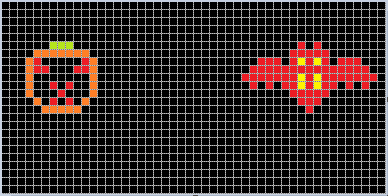
I’ve been working with my daughter Alice on an LED lightboard project for Halloween, and today we finished the construction. Whew! We started out two weeks ago with a giant 4 foot x 2 foot pegboard from Home Depot, and ambitious plans to make various Halloween shapes by populating specific holes. Reality quickly sunk in, though, as we realized how much work it would take to do something interesting with a 1152 hole pegboard. We eventually settled on building a much smaller 8 x 8 fully-populated LED matrix instead, controlled through software to make a variety of patterns and designs.
Even this 8 x 8 matrix was a lot of work, and for anyone contemplating a similar project, I’d recommend just buying a prebuilt LED display matrix like the Peggy 2LE instead. We probably could have found a simpler way to build the matrix, but it was a fun project nonetheless, and the result looks great. Take a look at the video, and then I’ll explain how it’s built.
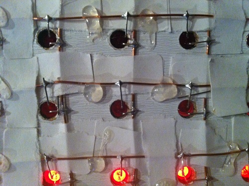
We started with a pegboard with 1-inch hole spacing, painted black on the front display side. Alice cut lengths of bare copper wire for the column busses, and lay them on the back of the board, just to the right of the holes. The bus wires were temporarily fixed in place using torn strips of adhesive tape. She then laid more bare wire on top to form the row busses, with additional layers of tape at the crossing points to ensure the row and column wires didn’t touch. The tape didn’t stick very well, so she reinforced the grid with hot glue, taking care not to cover the points where LEDs would be soldered later.
The next job was mine: building the controller circuitry. I used a MAX7219 LED driver, which is a nice (but expensive) single chip solution for controlling up to 64 LEDs. It handles all the multiplexing and storage of pixel values, so the microcontroller doesn’t have to do anything expect send SPI commands to change values when desired. The 7219 rapidly scans through the columns at about 800 Hz, activating each one in turn. This is fast enough that human vision sees them as being all active at once. The chip has sixteen driver pins: one for each row and column. It pulls one column high while the others float, and pulls rows low if the LED at that row/column intersection should be lit.
The 7219 can supply 320 mA to a column, which when divided by eight rows provides 40 mA per LED when the column is activated. Because the scanning action results in a 1:8 duty cycle for the columns, the average current per LED is only 5 mA. Typical current for an LED is about 15 mA, so 5 mA is fairly low. I was worried the display would look pretty dim as a result, but as you can see in the video, it’s actually quite bright.
I built the 7219 circuit on a piece of perfboard, hand-placing all the connections between the chip, row/column headers, control header, and power. What a mess! Whenever I build something on perfboard, no matter how simple, it always seems to turn into a giant mess with flakey connections everywhere. Unfortunately this example was no different. Soldering in the components is no problem, but I can never get the wires to stay put when soldering the connections. Any connection involving more than two wires is also a hassle. My pain with perfboards is why I favor manufacturing custom PCBs even for simple projects, but in this case there wasn’t enough time before Halloween.
With the control circuit ready, the final construction step was to populate the board with 64 LEDs. Alice and I took turns soldering and bending LED legs to shape. It was her first big soldering project, and she had a blast. It helped that everything had wide open joints to solder, and a mistake couldn’t do anything worse than kill a 10 cent LED. Populating the whole board took about two hours, working slowly and carefully through each joint.
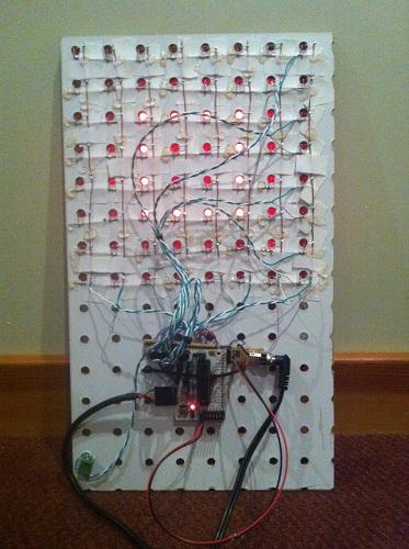
The finished board worked– sort of. It worked as long as you never lit more than 5 LEDs in a column, otherwise the display would go dark until you reset the Arduino. I wasn’t expecting this, but with my geek dad pride on the line, I had to find a solution.
My first thought was that this was some kind of clock glitch problem. I guessed that my terrible wiring combined with the sudden voltage swing from 6+ LEDs turning on was glitching the SPI clock. I spent some time fiddling with the clock wire and other control lines in an attempt to clean things up, to no avail. I also realized that a glitchly clock would likely produce display errors, but not make the screen go permanently dark, so I started looking for another explanation.
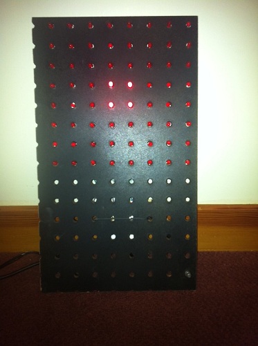
The display was finally fixed by reducing the current draw (and resulting brightness). The 7219 uses a current set resistor between two pins to control the current to the LEDs. I initially followed the sample circuit in the datasheet, using a 10K ohm resistor to provide maximum brightness. Through trial and error, I found that I had to increase the resistance to 30K before the display worked reliably. This should have resulted in a 3x reduction in current to the LEDs, but I only noticed a very minor reduction in perceived brightness.
Why was it necessary to use a larger set resistor? One possibility is that it was somehow drawing more than 320 mA with the original resistor, causing the 7219 to overheat or trip some kind of internal protection circuit. I can’t think what I might have done to make it draw too much current, though. A more likely explanation is that my shoddy power and ground wiring has a non-trivial amount of resistance, so when the current draw is high enough, +5V is pulled down and ground is pulled up far enough that either the Arduino or the 7219 no longer function. Either way, reducing the current fixes the problem, but one is a thermal problem and one is a supply voltage problem. I’ll leave further investigation for another holiday.
Now we need some cool animation displays for this board! Alice has been learning the basics of programming at Codecademy, and has already done some simple button-pushing and LED-blinking Arduino projects, so with a little help from me I think we can create a great-looking Halloween display.
Read 7 comments and join the conversationNewark/Farnell Product Review
It seems the Big Mess o’ Wires blog has reached the threshold where companies will send their products to be reviewed. I’m flattered. Newark (or Farnell for those of you in Europe, Element 14 in Asia) has kindly offered to send me a product of my choice from their catalog, anything 25 GBP (about $39) or less.
What kind of electronics parts are people interested in seeing reviewed? Tools? Development boards? Programmers? Kits? Specific ICs? My first thought was a demo board for one of the less common microcontrollers (not AVR or PIC), like the MSP430 or an ARM variant.
Check out www.newark.com, and post a comment if there’s something specific you’d like to see reviewed here.
Read 5 comments and join the conversationBuilding a Halloween LED Display
This Halloween, my daughter and I are working on a large LED display board for the yard. We started with a 3 x 6 foot pegboard with a grid of 24 x 48 holes pre-drilled, and 100 each red, orange, yellow, and green LEDs. 5mm size T 1 3/4 LEDs fit pretty nicely into the pegboard holes. Her job is to design some interesting animated shapes for the board, and my job is to figure out how to wire the whole thing up and power it.
My initial thought was to fill only the holes needed for a few specific Halloween shapes, and connect the LEDs using some ad-hoc point to point wiring. But the more I thought about measuring, cutting, stripping, and soldering hundreds of different ad-hoc wires, the more I hated the idea.
The Grid
Wiring up the board as a regular grid should be much easier, even if not all the grid points are used. The simplest method would be to lay down lengths of bare wire horizontally and vertically between the pegboard holes, using a plastic or rubber spacer at the crossing points to ensure the row and column wires don’t make electrical contact. To add a new LED to the grid, you’d just bend one leg down and solder it to the nearest row wire, and bend the other leg to the right and solder it to the nearest column wire. If the column wire was supplied a positive voltage while the row wire was grounded, then the LED at the intersection would illuminate. The great thing about this arrangement is that it wouldn’t require any wiring changes if you later need to change the shape of a jack-o-latern’s eye or a bat’s wing: you could just add a new LED to the grid, and alter the software that controls it.
Driving this grid would require 24 row lines and 48 column lines. The columns would be scanned rapidly one at a time, with all the row lines driven simultaneously to control the state of the LEDs in that column. If the columns were scanned rapidly enough, the human eye would perceive the whole display at once. The 24 row lines would most likely come from a shift register connected to the MCU, while the column lines would come from some type of decoder that enables exactly one of 2^N columns using N input bits from the MCU.
Splitting the Grid
Scanning through 48 columns one at a time would work, but with a 1/48 duty cycle, the LEDs would look very dim. A 1/8 or 1/4 duty cycle is more realistic in order to create an acceptably bright display. To achieve a 1/8 duty cycle, the grid would have to be divided into 6 independent sub-grids, each with 24 rows and 8 columns, with 192 LEDs per fully-populated sub-grid . Each of these sub-grids would require its own 24-bit shift register for the rows, and a 3:8 decoder for the columns.
Power requirements would likely force the sub-grids to be even smaller. Assuming 10 mA per LED, a fully-populated 24 x 8 sub-grid with all LEDs on would see 1.92 amps of current at the decoder, which is way too much for any common IC. After looking at some typical purpose-made LED driver chips, it looks like 300 mA is a more realistic upper limit.
I have a sample of the MAX7219 LED driver, which combines 8 row drivers and 8 column drivers with built-in column-scanning circuitry into a single chip. It can control 64 LEDs, with a total current limit of 320 mA. Each LED is driven with 40 mA when its column is enabled, and the 1/8 duty cycle results in an average drive current of 5 mA per LED. With 1152 total grid positions, it would require subdivision into 18 sub-grids to control the full grid with 18 MAX7219’s. For a brighter display, the MAX7219 could be configured with only 4 columns and a 1/4 duty cycle, for an average drive current of 10 mA per LED. That would require twice as many sub-grids and twice as many MAX7219’s.
Cost Estimate
At roughly $8 per MAX7219, the cost of driver chips would be $144 for the normal display, or $288 for the brighter display. That’s a bit out of the budget range for a weekend Halloween project! I suspect I could save a significant amount of money by using a simpler driver chip, but so far a specific solution has eluded me. The row drivers need constant current outputs, with a relatively high current limit in the 40 mA range. The column drivers (assuming they’re a separate chip and not combined like the MAX7219) need a very high current limit in the 300+ mA range.
The best option I’ve found for the row drivers is the STP08DP05B1, a $1.82 chip with eight constant-current outputs able to supply up to 100 mA per row and 800 mA total. I’m having a little trouble understanding the datasheet, though, and I’m not certain those are truly the per-pin current numbers, and whether they’re for sourcing or sinking current.
I’ve not yet found any good options for the column drivers, probably because I don’t know what such things would be called. High-power decoders? Analog demux switches? I need something with three digital inputs, that enables one of eight analog outputs, and can supply as much current as possible to that output, but at least 300 mA.
I could also use standard low-power shift registers and decoders, connected to separate high-power transistors. That would greatly increase the total number of components needed, though, since I’d need a separate transistor for every row and column in every sub-grid.
No matter what the eventual solution, it appears the cost for driver electronics will be at least $50 or so, and possibly much more.
Power
The power requirements of the full grid would be non-trivial. Assuming I used 18 of the MAX7219 drivers, the maximum current draw would be about 6 amps! That’s well outside the capability of any wall-wart 5V supply in my collection, and would probably require some type of bench supply or switching power supply scavenged from an old PC. However, the display would only draw 6A if it were fully populated with all LEDs simultaneously turned on. With a less than fully populated grid, and some upper limit on the fraction of LEDs that could be on at once, the power requirements might be reduced to a more reasonable level.
Solutions?
Since I’m not about to give up on this display entirely, nor wire up a few hunded LED’s with ad-hoc point to point wiring, some variation of the grid approach looks like the only viable solution. That means I’ll be spending a lot of money on driver electronics and a high-current power supply. To help keep the cost and assembly time down, I’ll probably only build a subsection of the entire 24 x 48 grid, but do it in a way such that the rest of the grid can be populated over the course of future holidays. 🙂
Edit: Thinking about this further, I’m starting to doubt whether this project is a very good idea. 5mm LEDs with a 1 inch grid spacing will do a very poor job of space filling, so this display likely won’t look very good. It will appear more like a bunch of isolated point lights than adjacent pixels in an image– OK for abstract displays, but not so good for making a recognizable image of a jack-o-lantern.
My bigger concern is safety. Combining a 6A power supply with a grid of bare wires on the back of the board sounds pretty dangerous. Curious fingers could get a significant shock.
Read 5 comments and join the conversation