

Archive for the 'Dev Tools' Category
FPGAngst
I’ve spent the past few days getting familiar with my Xilinx Spartan 3A Starter Kit, and so far, it’s not going well. I’d thought I was pretty competent with the basics of digital electronics, and the concepts of HDL programming and FPGAs. But working through a “blink the LED” example using the Xilinx ISE WebPack software has been an exercise in frustration. The learning curve is more like a brick wall, and I’m getting dizzy from banging my head into it over and over.
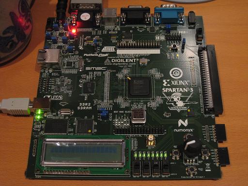
I’ll begin with the starter kit itself. Given the name, you might think it’s aimed at people who want to get started with FPGAs. Forget it. I was very disappointed to find that the starter kit came with almost no documentation at all. Instead, it just had a DVD with a two year old version of the ISE software (now two major releases out of date), and a leaflet with a URL to find more information. The only printed documentation was for the Embedded Devlopment Kit, which is a separate product and doesn’t even work with the free version of the Xilinx ISE. Following the URL, I found the manual for the starter kit, but it’s little more than a catalog of all the hardware on the board. If you want any kind of tutorial for an FPGA “hello world” using this board, or a high-level overview of the various steps involved in creating and programming an FPGA design, or any kind of “starter” information at all, you’ll have to look elsewhere.
Plowing through the ISE software on my own, the first issue I faced was the need to choose what FPGA model I wanted to target. You might think there would be a predefined choice for “Spartan 3A Starter Kit”, but you’d be wrong. After some digging, I found that the starter kit has a XC3S700A, but that wasn’t enough. I needed to specify what package it was, and what speed grade too. How do you tell this? It’s mentioned nowhere in the starter kit manual. After about 20 minutes of searching around, I finally managed to find the web page that deciphered the tiny, near-illegible numbers printed on the chip to determine the package and speed. It’s FG484-4, if you’re keeping score at home.
The ISE itself is really bewildering. It’s basically a shell application that coordinates half a dozen other tools, each of which has its own UI and terminology. The other tools look like old command-line apps that someone slapped together a GUI for using Tcl/Tk. The ISE uses a strange (to me at least) “process” metaphor, which is a context-sensitive subpanel that fills with different actions, depending on what you’ve selected in the main GUI. It took me two days of hunting to figure out what I needed to click on to make the simulation-related process options magically appear. The processes are also arranged in a hierarchical list, so in most cases, running a process requires running all the ones in the tree before it. I still haven’t figured out how to check if my Verilog compiles without doing a complete synthesize, place, and route for the entire design.
Other ISE headaches:
- The GUI-based Plan Ahead tool used to assign signals to physical pins bears no relation to the text-based UCF (user constraints) file examples in the starter kit online manual.
- ISE keeps getting confused about the UCF file, and I have to remove it from the project and re-add it. It’ll complain that I don’t have a UCF file, then when I try to add one, it complains there already is one.
- Integration with iMPACT (the programming tool) is apparently broken. ISE says it’s launching it, but doesn’t. iMPACT must be launched manually.
- After using a wizard to create a DCM module to divide the input clock by two, there’s no “results” page or other info that defines what ports the wizard-created module has. It doesn’t let you actually look at the module code: clicking on it just relaunches the wizard. I had to go poke through random files on disk to discover the module ports.
In comparison to the software, the hardware itself seems pretty good, but maybe a little TOO good. There are no less than four different configuration EEPROMs that can be programmed, with a complicated system of jumpers for controlling which one to program and which to use at startup. This just makes life more complicated than it needs to be.
The only big negative about the hardware is that there’s no SRAM at all. I don’t know how I missed this when I was looking at the specs. Instead, it has 64MB of DDR2 SDRAM. Yeah, that’s a lot of RAM, but creating a memory controller interface for DDR2 RAM is a big honking complicated task all in itself. That means that if you want to do any kind of project involving RAM, you either need to be content with the few kilobytes of block RAM in the FPGA itself, or go on a long painful detour to design a DDR2 memory controller first. The 133MHz oscillator for the DDR2 RAM also occupies the only free clock header, so it’s impossible to introduce another clock to the design (for example, a 25.175MHz oscillator for generating VGA video).
Stumbling blindly through the software, I did finally manage to design, simulate, program, and run a simple example that blinked three LEDs. I’m sure everything will make more sense in time, but it’s hard for me not to feel grumpy right now. I feel like I’m spending all my energy wrestling with the tool software, and none on the project itself. In short, it feels like a software project, not a hardware one. I’ve barely touched the board, other than to plug in the USB cable and flip the power switch. My multimeter, chip puller, wire stripper, and other tools sit unused in my toolbox. Instead, I’m spending time reading a lot of manuals and guessing at what some opaque piece of software is actually doing under the hood. The experience with the clock generation wizard was downright depressing: it just writes some HDL code for you and doesn’t even let you see it, so you’re at least two levels removed from having a prayer of actually understanding what’s going on. Since my end goal in all my homebrew hardware is to gain a better understanding of how things work, that’s especially galling.
I’m going to search out some more ISE tutorials and any other good learning tools I can find, but I’m also going to take another look at the Altera tools. I’ve heard that the Altera software is more beginner-friendly, but I went with Xilinx becuase their starter kit appeared more powerful. I’m now realizing that the quality of the software tools and ease of the development experience is much more important than the number of gates on a particular FPGA. Altera’s Cyclone II starter kit isn’t as full-featured as the Xilinx kit I have now, but it’s decent, and it has some SRAM too. More than likely, the Altera tools will just be a different flavor of incomprehensibility, but it’s worth a look.
Read 37 comments and join the conversationFun With Dremel
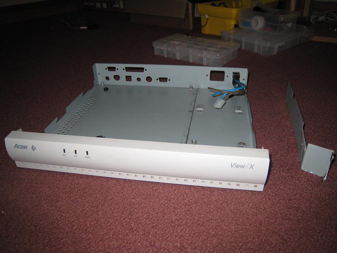
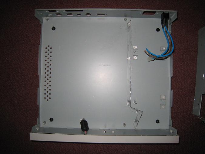
A while ago I purchased an old X-terminal and ripped out the guts, with the intention of using the case for BMOW. Upon opening it up, I discovered that the interior was partitioned into two parts by a steel divider welded to the base. The logic board was on one half and the power supply on another. Unfortunately BMOW needs the entire space in order to fit its oversized board.
Enter the Dremel tool. I got a Dremel and assortment of attachments for Christmas, but didn’t have a chance to try it until today. My plan was to simply cut the divider off, requiring about a 12 inch cut. The divider is made of 1/32 inch steel. Would the Dremel cut it? What kind of cutting attachment should I use? Would I slice off a thumb? I really had no idea how to use a Dremel, but a couple of the included attachments looked like cutting wheels, so I gave them a try. It took me about an hour and a half to make the 12 inch cut, and it looks pretty darn ragged, but the operation was a success. Sparks were flying everywhere… it was quite a sight! I ate up two entire cutting wheels, though, so I’m guessing a wheel made specifically for cutting steel would be better next time.
Here’s my handiwork. You can see the stump of the divider running from the case’s front to its back, about two-thirds of the way from left to right.
I had hoped to cut a large hole in the case lid, and cover it with a piece of plexiglass, to make a window where people could peer in and see BMOW’s guts. Given how this cut turned out, though, I think I’m going to abandon that idea. It would probably take me several hours to make a hole that large, and it would end up looked pretty ragged and ugly. Instead, I’ll just pop the lid when I do demos!
Read 7 comments and join the conversationCustom PCBs
While I wait for my new audio power amp chips to arrive, I’ve started looking at making a custom PCB or two for BMOW’s various buttons, connectors, and jacks. I plan to use a pizza-box case from an old X-terminal that’s the perfect size, and already has case cut-outs for VGA and keyboard connectors, and other goodies. I could try to use all panel mount connectors with wires running back to the BMOW board, but some parts like the VGA and keyboard connectors typically only come in PCB-mount varieties.
I plan to design a simple PCB of about 1×5 inches, which will hold the various connectors, as well as the audio amplifier and related circuitry. It will be a long narrow board mounted in the back of the case, right next to the cut-outs, with headers for connecting cables internally back to the BMOW board. Of course I don’t really need to do this, but it’ll help make everything look neat and professional, and I’ve been looking for an excuse to design a PCB for a while. I know nothing at all about the design process, but I’m interested to learn. I will definitely keep this to a 2-layer or even 1-layer design, to keep it as simple as possible.
I wrote a little bit about some PCB manufacturing options in a comment to a posting last summer: /2008/08/17/wire-wrapping-pain . At this point I think I’ve narrowed the choices to ExpressPCB and their free, proprietary CAD tools, or the free version of Eagle PCB and Futurlec’s manufacturing service.
ExpressPCB looks very easy to use, and easy to submit designs, with very quick turn-around on manufacturing and shipping. That’s pretty important, because I’m notoriously impatient. Their “miniboard” package gives you three copies of a 3.8 x 2.5 inch board for $51 plus shipping. Unfortunately their software seems pretty basic, and its built-in library of components isn’t great. It also locks you in to their proprietary file format, with no easy way to export your design to other programs and manufacturers later.
Eagle PCB seems to be the standard tool for hobbyists making PCBs. It looks more full-featured, but with a steeper learning curve for newbies like me. The free version has a size limit of 8×10 cm (3.9 x 3.1 inches). Futurlec will accept Eagle files, and turns around orders in 7-10 business days. The cost for a single board comparable to ExpressPCB’s miniboard is $31, or $43 for three of them, plus shipping. They’re in Thailand, but were able to ship my last parts order to me in just two days, and it had some cool elephant stamps on the package to boot.
Given these size constraints compared to my desired 1×5 board size, I’ll probably try to design a board with half the connectors on one side and half on the other, and get two of them. Then I’ll put the two boards side-by-side with one rotated 180 degrees, and populate half of each board with the appropriate connectors. It’ll be two 3.8 x 1.25 logical boards sharing each 3.8 x 2.5 physical board.
I’m leaning towards Eagle PCB + Futurlec, but I plan to play around with them both for a while, and see what sticks. It should be fun!
Be the first to comment!Logic Analyzer/Oscilloscope
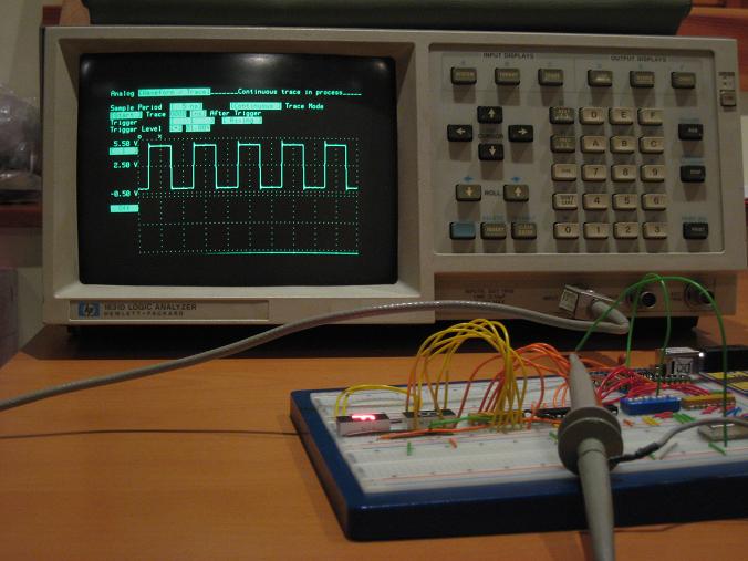
My Hewlett-Packard 1631D logic analyzer / digital oscilloscope arrived today: the finest 1985 technology that $35 can buy. I bought it dirt cheap from eBay in “as is” condition, but it seems to be working great! With this acquisition, I can proudly say that I’ve crossed the line from ordinary run-of-the-mill nerd to super-nerd.
Holy cow, there are a lot of buttons and wires on this thing. What’s a trigger? Where’s the manual? My head hurts just thinking about it.
After some time spent jabbing hesitantly at buttons, I finally managed to get a scope trace working. Here it is, showing the output of a 1 MHz clock oscillator. Mmmm, square wavy goodness!
Universal Programmer
I got a TOP 2007 universal programmer yesterday, for burning EPROMs, GALs, and Flash memory. Whenever I hear the term “universal programmer”, I imagine a nerd-equivalent of the 1992 movie Universal Soldier, starring Jean-Claude Van Damme. Plot: a mild-mannered C++ programmer gets cybernetic implants and goes on a killing spree.
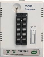

TOP 2007 Pros: It’s pretty cheap (about $100), and it programs GALs, unlike most low-cost programmers.
TOP 2007 Cons: Horrible, horrible software. I’ve seen slipshod, poorly-translated software before, but this really elevates it to an art form. Maybe 25% of the text isn’t translated at all, and is still in Chinese, including some status and error messages. What text is in English is so poorly translated, it’s difficult to tell what it means. “Driver not ready ,if load it now?” Damned if I know. And what’s a “cussor?” Clicking the close box minimizes the window instead. Reading from a chip overwrites the contents of any data file you previously had open for writing. Lots of options and menu items do mysterious unknown functions, or nothing at all. Device recognition doesn’t seem to work– you have to manually select the right device from a list of hundreds, and pray you got it right.
Despite these issues, programming a 128K Flash memory worked fine. I had problems with some Lattice 22V10D GALs, however. That’s especially frustrating, since GAL support is the whole reason I chose the TOP 2007 over other choices. The 22V10 is on the supported device list, and it does almost work, but not quite. What appears to happen is that it successfully programs all the 5000+ fuses needed to implement the logic expressions, but won’t program the last 20 fuses that configure the output pins to be inverting or non-inverting, registered or combinatorial.
Any sane person would have attempted to return the programmer, or junk it and get a better one. Instead I spent an afternoon trying to reverse engineer the software to see if I could fix the problem. By accident, I discovered that I could program 14 of the 20 unprogrammable fuses by adding extra fuse data to the data file, beyond the number of fuses that are actually in the GAL. I also found that 3 more of those 20 seemed to copy the data from elsewhere in the fuse map. But the last 3 fuses appear permanently stuck at 0. The net result is that with some complicated effort, I can completely configure 8 of the 10 GAL outputs. The other two are stuck in registered, inverting mode. I can probably work with that for most purposes. Worst case, those 2 outputs will just be unused.
GAL Counter: The hardware design calls for a stack pointer that’s a 24-bit up/down counter with output enable. The simplest approach would be to use six 4-bit up/down counters, and three 74LS244 drivers, requiring nine chips total. A better solution would use the hard-to-find 74LS569 4-bit up/down counter with integrated output enable, requiring only six chips. Better still would be to use three 22V10 GALs to make 8-bit up/down counters with output enables, requiring just three chips.
It turns out that programming an 8-bit up/down counter into a GAL is quite a challenge. For starters, there are barely enough pins. The 22V10 has 22 data pins, of which at most 10 can be outputs. I was able to barely cram it in by encoding some of the control inputs into a 2-bit function code. But the bigger challenge is that the logic equations for computing the new value of each counter bit require more product terms than the GAL supports. My equation for the MSB of the counter includes 19 AND terms all OR-ed together, but the 22V10 supports at most 16 terms. Here’s my equation:
/q7 := f1*f0*/q7 + /f1*/cet*/q7 + f1*/f0*/d7 + /f1*f0*cet*q0*q1*q2*q3*q4*q5*q6*q7 + /f1*f0*cet*/q7*/q0 + /f1*f0*cet*/q7*/q1 + /f1*f0*cet*/q7*/q2 + /f1*f0*cet*/q7*/q3 + /f1*f0*cet*/q7*/q4 + /f1*f0*cet*/q7*/q5 + /f1*f0*cet*/q7*/q6 + /f1*/f0*cet*q7*/q6*/q5*/q4*/q3*/q2*/q1*/q0 + /f1*/f0*cet*/q7*q0 + /f1*/f0*cet*/q7*q1 + /f1*/f0*cet*/q7*q2 + /f1*/f0*cet*/q7*q3 + /f1*/f0*cet*/q7*q4 + /f1*/f0*cet*/q7*q5 + /f1*/f0*cet*/q7*q6
cet is the count enable (active high). F=00 means count down, F=01 means count up, F=10 means load, and F=11 means no change. So this crazy equation says that bit 7 should be zero if we’re not changing and the current bit 7 is zero, or we’re trying to count up/down but counting is disabled and the current bit 7 is zero, or we’re loading and the input bit 7 is zero, or we’re counting up and the counter is at 11111111, or we’re counting up and the the current bit 7 is zero and any of bits 0-6 are zero, or we’re counting down and the counter is at 10000000, or we’re counting down and the current bit 7 is zero and any of bits 0-6 are one. Phew! If you can simplify that to 16 product terms, you’ll win a prize. Maybe I should create a truth table with 4096 entries, and build a Karnaugh map. Or not.
I need to take another look to make sure there isn’t some clever way I can simplify the equation to get under 16 terms. If not, then I’ll probably either make four 6-bit up/down GAL counters (which would be a little strange, since bytes would be awkwardly divided among different GALs), or six 4-bit up/down GAL counters, essentially replicating a 74LS569 in a GAL. So far I haven’t found any place that has 74LS569s is stock.
Read 5 comments and join the conversation