Archive for the 'Floppy Emu' Category
ProDOS Software Collection for Floppy Emu
Craig of apple-2.com has put together a great collection of Apple II software with a Floppy Emu theme. It’s a 32 MB bootable ProDOS disk image with an animated splash screen, and it uses the amazing Bitsy Bye program launcher to select from a variety of included games and utility programs.
Floppy Emu can use this disk image to boot your computer, when the Emu is configured for Smartport hard disk emulation mode. Just rename the disk image to SMART0.PO and copy it to your SD card. It’s compatible with the Apple IIGS, Apple IIc and IIc+, and Apple IIe with Liron card.
Craig cautions that some of the included games like CANNON.BLITZ may not work correctly when launched directly from Bitsy Bye, due to a memory conflict. If you find a game that crashes when run from Bitsy Bye, reboot and select GAMES.CATALOG from within Bitsy Bye. Then type in “-CANNON.BLITZ” or “BRUN CANNON.BLITZ” and the game should run normally.
Download the disk image here: SMART0.PO
Don’t forget to check out apple-2.com’s other vintage download collections.
Be the first to comment!Get 10 Give 10 – Floppy Emu and Samaritan House
![]()
Looking for a discount on a Floppy Emu Deluxe Bundle, and want to spread some holiday cheer at the same time? BMOW is running a holiday promotion called Get 10 Give 10. Use the coupon code GET10GIVE10 during checkout, you’ll save $10 off a Floppy Emu Deluxe Bundle, and I’ll donate a further $10 to Samaritan House of San Mateo. It’s a chance to save money on retro computer hardware and do something good for the world too.
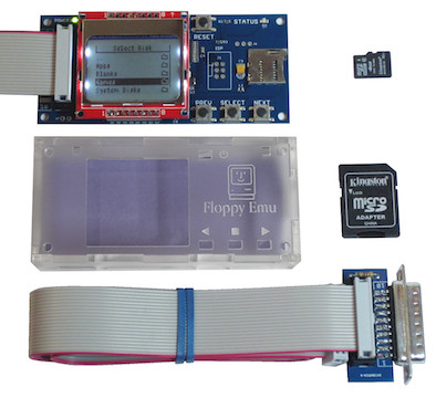
Floppy Emu is a floppy and hard disk emulator for classic Apple II, Macintosh, and Lisa computers. It uses an SD memory card and custom hardware to mimic an Apple floppy disk or hard disk drive. It’s perfect for booting your favorite games, transferring files from vintage to modern machines, and troubleshooting a computer without a working OS. The deluxe bundle includes the Floppy Emu, an acrylic case, and an SD card with a collection of vintage Apple software disk images. Full details are available here.
Samaritan House provides food, shelter, healthcare, housing, financial assistance, and more to low-income and homeless persons in the San Francisco Bay Area. Even in the midst of Silicon Valley’s affluence, there are many people struggling just to meet the basic needs of daily life. A small boost at the right time can help them regain self-sufficiency. Samaritan House operates a broad variety of free services and one-on-one assistance with caring staff. I’ve seen first-hand what they can do, and it’s amazing.


If you’ve had your eye on a new Floppy Emu, or need a second or third unit for your growing computer collection, here’s your opportunity. Thank you for supporting the good work of Samaritan House!
Enter the coupon code GET10GIVE10 during checkout to take advantage of this offer.
Read 2 comments and join the conversationApple IIc Drive Switcher Back in Stock
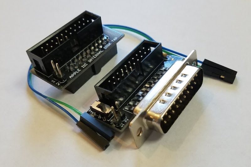
The Internal/External Drive Switcher for Apple IIc is once again available in the BMOW Store. The Switcher is a convenience option for Floppy Emu owners with a IIc, and makes everything easier when when emulating a 5.25 inch floppy disk drive. It provides a simple way to select whether the internal floppy drive or external Floppy Emu will appear as 5.25 inch Drive 1, which is the only bootable drive on the IIc. More details are here.
Be the first to comment!Limiting SD Card Inrush Current
I’m experimenting with methods to limit the inrush current when an SD card is inserted, and beginning to wonder whether my solutions are worse than nothing.
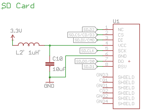
When an SD card is inserted into a board that’s already powered on, a large amount of current will flow briefly, as the card’s internal capacitors are charged through its 3.3V supply pin. This is called inrush current. If the inrush current is too large, it can overtax the main board’s voltage regulator and capacitors, causing the board’s supply voltage to drop temporarily. If the voltage drops far enough, it may cause the board’s microcontroller to do a brownout reset. That’s what happened with early versions of the Floppy Emu. It wasn’t really a problem, because you’ll almost always want to perform a reset anyway after inserting a new card, but it was slightly annoying.
In later versions of the Floppy Emu, I added a 1 uH inductor and 10 uF capacitor for the SD card, as shown in the circuit schematic above. Later the capacitor was changed to a 33 uF tantalum. The purpose of the inductor was to limit the inrush current, preventing the main board’s supply voltage from sagging and causing a brownout. And it worked, mostly, as confirmed by observing the main supply and SD card supply voltages on a scope during card insertion. The exact behavior depended on the brand and type of SD card and the card’s internal circuitry. Some types of cards still caused a brownout reset when hot-inserted, but it was rare.
Revisiting this question again recently, I noticed that the inductor created a new issue that may be worse than the one I was trying to solve. When the SD card is inserted, its 3.3V supply pin doesn’t go cleanly from disconnected to connected. Instead it bounces and wiggles over a period of microseconds to milliseconds, just like the contacts of a mechanical switch. As a result, the inrush current isn’t one single burst, but a series of short on/off current pulses. Because of the presence of the inductor in the circuit, these pulses create voltage spikes on the SD card’s 3.3V supply pin. They’re brief – lasting about 100 ns – but some of the spikes go above 4V. Despite their brevity, I’m wondering if they’re high enough to damage the SD card.
Using an inductor seems to be a pretty standard solution for SD card inrush current, but I’ve never seen any discussion of the voltage oscillation and spikes this can cause for the card’s supply. An alternative is a power management IC with “soft start” behavior, but I’m not interested in adding extra chips in this case. I’m starting to think it may be best to remove the inductor, and connect the card’s 3.3V supply directly to the board’s 3.3V supply. Better to cause a nuisance brownout due to high inrush current, than to risk damaging the card with voltage spikes – and still have brownouts sometimes anyway. Have you ever dealt with this topic? How did you address it?
Read 16 comments and join the conversationApple IIc Drive Switcher Version 2
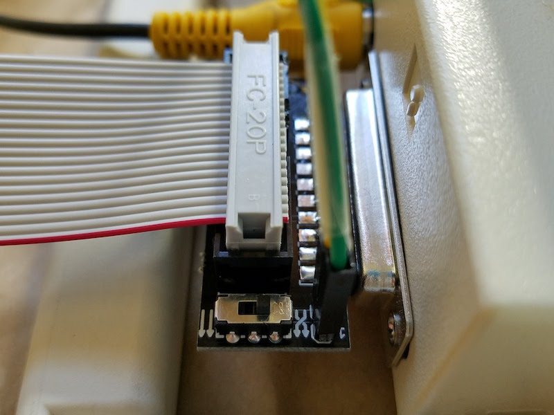
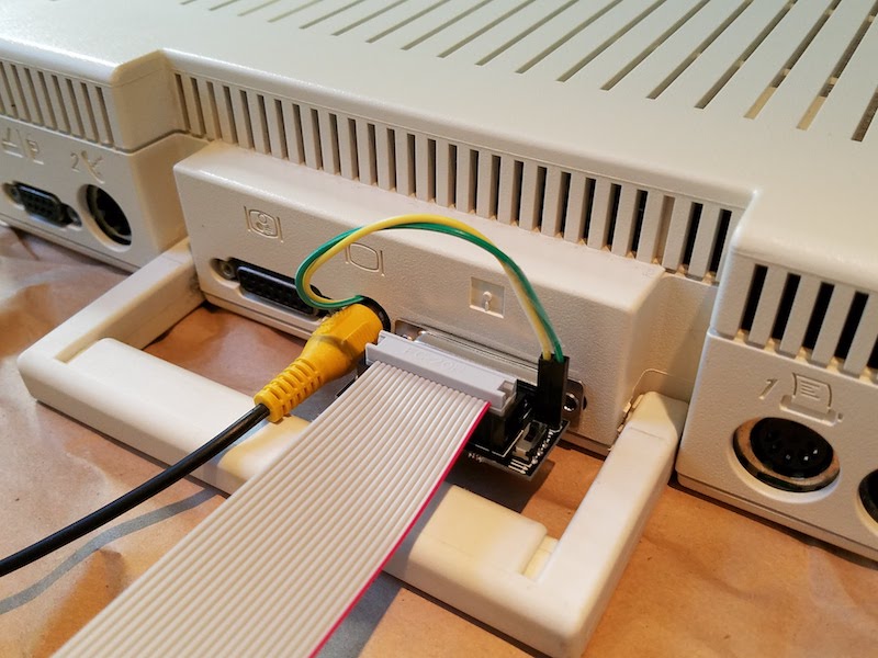
Version 2 of the Apple IIc Internal/External Drive Switcher is here, and is working nicely. It’s mostly the same as version 1, except for a few tweaks to the piece that goes inside the IIc case. Although the inside fit is still very tight, with this new version it’s a little more forgiving. I also updated the switch labels on the external portion of the drive switcher, with an icon showing parallel arrows for normal mode, and crossed arrows for drive swap mode.
In my previous trials with the drive switcher, I threaded two wires through a gap in the Apple IIc case around the 19-pin disk port. That works, but I’ve concluded it’s easier to thread the wires through the gap around the composite video connector instead, as shown in the photo below. There’s a little bit more wiggle room, and it avoids blocking the faceplate of the male DB-19 connector when the external portion of the drive switcher is plugged in. Threading the wires around the video connector doesn’t cause any blockage problems, and I had no difficulty plugging in the video cable. You could also thread the wires around the DB-15 monitor port, which most people aren’t using anyway.
I think it’s ready! Now I just need to assemble a few of these and get them ready for sale. If you’re interested in helping to beta test the first few units, please let me know.
Read 14 comments and join the conversation10000 More DB-19 Connectors

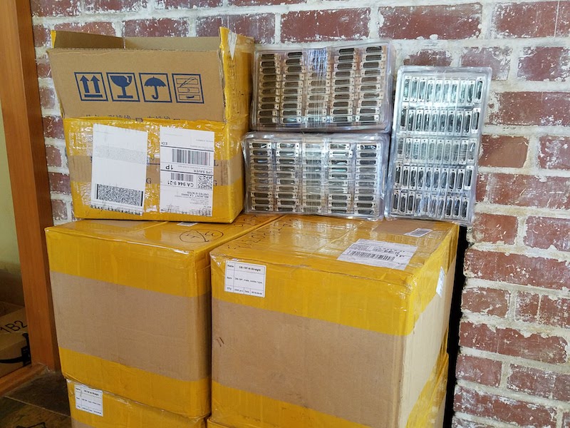
Oops, I did it again: another 10000 DB-19 connectors fresh from the factory! After helping to resurrect this rare retro-connector from the dead in 2016, and organizing a group of people to share the cost of creating new molds for manufacturing, I had some of the 21st century’s first newly-made DB-19s. The mating connector is found on vintage Apple, Atari, and NeXT computers from the 1980s and 1990s, so having a new source of DB-19s was great news for computer collectors.
But that was two years ago. After manufacturing, the lot of connectors was divided among the members of the group buy, leaving me with “only” a few thousand. Since then I’d used up more than half of my share in assembly of the Floppy Emu disk emulator, and I began to get nervous about the looming need for a re-order. It was such a big challenge the first time finding a Chinese manufacturer for the DB-19s, and the all-email company relationship was tenuous. What if they lost the molds? What if my contact there left the company? What if the company went out of business? Even though I didn’t absolutely need more DB-19 connectors until 2019 or 2020, I decided to lock in my future supply and order more now.
I needn’t have worried, and the transaction went smoothly. With no mold costs to pay this time, the only challenge was meeting the 10000 piece minimum order quantity. I was even able to pay via PayPal, instead of enduring the hassles and weird scrutiny of an international bank wire transfer like I did in 2016.
So now I have a near lifetime supply of DB-19 connectors. Call me strange, but it actually gives me a warm fuzzy feeling. Now to find someplace to store all these boxes…