

Archive for the 'Plus Too' Category
Hardware Simplification
Today I’ve been thinking about ways to simplify the Plus Too hardware. Anything I can do to reduce the part count will make the final board easier to build, and also help with the the inevitable debugging work. The nice thing about some of these ideas is that they dovetail, making further simplifications possible.
Soft-68000
My original plan was to use a real 68EC000 CPU. My motivations were a desire for “design purity”, and a wish to avoid having to learn how to work with a 68000 FPGA core and its possible bugs. After experimenting a bit with the free TG68 core, however, I’ve completely changed my mind. It took me just 30 minutes from downloading the TG68 files to having a working 68000 executing instructions from the Macintosh ROM inside my FPGA. The design is much easier to understand than I’d expected, and my fears of configuration voodoo and weird bugs seem unfounded. Using TG68 will not only allow me to eliminate a chip, but will also make it possible to directly inspect CPU registers and perform other live debugging tricks that wouldn’t be possible with a physical 68000 CPU.
One FPGA
In my earlier Too Many Pins entry, I counted the number of required FPGA I/O pins, and concluded I either needed to use two separate FPGAs, or learn how to solder BGA components. It turns out that most of the I/O pin count was related to connections to the physical 68000 CPU. I recounted the I/O pin requirements assuming the use of TG68, and it’s only 58 pins, plus or minus a few that I probably forgot. That’s well within the user I/O count of a single FPGA in a TQFP package, which I have some hope of hand-soldering. So there’s another chip gone.
Configuration by Microcontroller
Unlike the CPLDs I’ve used before, FPGAs don’t maintain their configuration when the power is turned off. They must be reloaded with the configuration bitstream each time they’re powered up. Although I didn’t call it out specifically, I had assumed the FPGA configuration data would be stored in a standard configuration Flash ROM. These ROMs are programmable through JTAG, and have all the smarts needed to configure the FPGA.
Some reconfigurable computers like Minimig use a different technique, and store the bitstream in an alternate medium, using a microcontroller to read the bitstream data and configure the FPGA. Because Plus Too will already have a microcontroller for floppy disk support, and an SD memory card loaded with floppy disk images, it should be possible to use the microcontroller to load the FPGA configuration bitstream from the SD card. I haven’t investigated the details yet, but with some good examples already out there, I’m hoping that it won’t be too difficult to get working.
ROM image in RAM
Taking this same idea one step further, the Macintosh ROM data could be stored in another medium, and loaded into a section of RAM at initialization time. The transfer of the ROM image could probably be done by the microcontroller, or else by a module in the FPGA that runs before the TG68 soft-CPU module starts. Assuming a large enough RAM, both the “real RAM” and the ROM image could exist side-by-side. The address decoder would direct accesses in the ROM address space into an alternate section of RAM, and ensure that all accesses to this section were read-only.
And Then There Were Three
If you put all these ideas together, only three chips remain: an FPGA, a microcontroller, and a RAM. Three main ICs to solder sounds very manageable. The other components are miscellaneous parts like the clock oscillator, buttons and LEDs, and some discrete components for video and audio output. Of course there will still be quite a few connectors to solder: the SD card holder, PS/2 jacks, VGA port, JTAG connector, serial connector, and maybe some others I’m forgetting.
Three’s a Crowd?
To simplify things still further, it might be possible to eliminate the microcontroller, and implement a microcontroller soft-core in the FPGA instead. Free cores for the ATmega instruction set and other microcontrollers already exist. This raises the question of where the microcontroller program and data are stored, however, as both are too big to be implemented inside the FPGA. Perhaps they could live inside the RAM alongside the CPU’s RAM and Macintosh ROM image, but then the microcontroller would contend with the CPU for memory access. Eliminating the microcontroller would also require reintroducing some other part to configure the FPGA at initialization time, so there would be no net component savings. For all these reasons, it doesn’t seem that eliminating the microcontroller would help.
Read 5 comments and join the conversation
Understanding Verilog Warnings
Those of you who’ve followed the blog for a while know about my many frustrations with Verilog. Because it feels sort of a like a procedural programming language, but very definitely isn’t one, I keep expecting to be far more competent at Verilog design than I actually am. While working on Plus Too, the Xilinx synthesis tool reported many, many warnings that I didn’t understand. The warning list grew to at least 100, and was so long that I just stopped reading it. That was dangerous, as most of the warnings were likely problems that needed to be addressed.
I’ve been writing C and C++ programs for years, and I’m very comfortable with the language, its details, and the compiler warnings and errors produced by various mistakes. I normally find the warnings easy to understand, because they reference a specific file and line number, and use well-known terminology to describe the problem. Sure, some more obscure errors like “not an lvalue” would probably flummox a beginner, but at least he’d know what line to scrutinize.
Most Verilog warnings I see are non-localized, and do not reference a specific file or line number. They are design-wide warnings, resulting from an analysis of all the modules in all the .v files. This can make it unclear where to even being looking for the cause of a warning. A typical example is something like:
Xst:647 – Input <vblank> is never used. This port will be preserved and left unconnected if it belongs to a top-level block or it belongs to a sub-block and the hierarchy of this sub-block is preserved.
OK, there’s an unused input named vblank. But where? The vblank signal is routed through half a dozen different modules in the design, so how do I know which one I messed up? The only solution I’ve found is to search the whole project for all references to vblank, and verify each one. I also find that error message much too wordy.
Another example:
Xst:646 – Signal <ramAddr<0>> is assigned but never used. This unconnected signal will be trimmed during the optimization process.
This is basically the same as the first example, but has a totally different warning message. Why? Because one is single combinatorial output, and one is a bit in a register? Then there’s this:
Xst:2677 – Node <ac0/vt/videoAddr_17> of sequential type is unconnected in block <plusToo_top>
It’s essentially the same issue again, but yet another totally different warning message. This time it gives the name of the offending module, so it should be easier to track down.
The general meaning of all these warnings is fairly clear: some expected signal connections are missing. Find the problem, and either add the missing connection, or suppress the warning if the unconnected signal is intentional. There were two other warnings I saw frequently whose meanings were definitely not clear to me, however:
Xst:2042 – Unit dataController_top: 34 internal tristates are replaced by logic (pull-up yes): cpuData<0>, cpuData<10>, cpuData<11>, cpuData<12>, cpuData<13>, cpuData<14>, cpuData<15>, cpuData<1>, cpuData<2>, cpuData<3>, cpuData<4>, cpuData<5>, cpuData<6>, cpuData<7>, cpuData<8>, cpuData<9>, mouseClk, mouseData, ramData<0>, ramData<10>, ramData<11>, ramData<12>, ramData<13>, ramData<14>, ramData<15>, ramData<1>, ramData<2>, ramData<3>, ramData<4>, ramData<5>, ramData<6>, ramData<7>, ramData<8>, ramData<9>.
Um, what? This meant nothing to me. I wasn’t even sure if replacing internal tristates with logic was good or bad. The Xilinx tool shows each warning as a link you can click to get more info, but sadly it doesn’t work. Clicking the link just opens a web browser and does a search on the Xilinx site for “Xst:2042”, which returns no results. In fact, none of the synthesis warning links work. If a warning doesn’t make sense to you, you’re on your own.
After a lot of searching around on other web sites, I finally found a decent explanation. It seems that some (or all?) Xilinx devices do not support tristate logic (a signal with an output enable) anywhere but on the actual I/O pins. Signals internal to the FPGA can not be tristate. Tristate logic is typically used to enable multiple drivers to operate on a single shared bus, one at a time. So instead of using internal tristates, you need to construct your design using additional logic to select which module’s data should appear on the shared internal bus, using a mux or similar method.
That mostly makes sense, but I’m using the FPGA to simulate a system of separate parts (address controller, data controller, CPU, RAM, etc) that will eventually be physically separate chips communicating with tristate logic on shared busses. I don’t want to rewrite my design to eliminate tristate logic, because tristate logic is what will be used for these chips. For now I’ve left the logic as is, and I’m ignoring the warnings, and it seems to be working OK. I’m unclear exactly what the synthesis tool has substituted for the internal tristates, though– “logic (pull-up yes)”? What is that, and what problems might it cause?
The other confusing warning that’s been plaguing the design is:
Xst:2170 – Unit plusToo_top : the following signal(s) form a combinatorial loop: ramData<0>, ramData<0>LogicTrst20.
Xst:2170 – Unit plusToo_top : the following signal(s) form a combinatorial loop: ramData<1>, ramData<1>LogicTrst20.
…
…and so on, for every bit of ramData. This stems from my attempt to specify a bidirectional bus driver akin to a 74LS245:
assign ramData = (dataBusDriverEnable == 1’b1 && cpuRWn == 1’b0) ? cpuData : 16’hZZZZ;
assign cpuData = (dataBusDriverEnable == 1’b1 && cpuRWn == 1’b1) ? ramData : 16’hZZZZ;
This driver has ramData on one side, and cpuData on the other. When it’s enabled, it drives data from one side to the other. The direction in which data is driven is determined by the cpu read/write line. So why does this form a combinatorial loop? I’d expect to see that warning for something like:
assign a = b & c;
assign b = a & d;
but my bus driver code looks OK to me. I still haven’t found an explanation for this one, but I think it’s related to the previous issue about internal tristates. The synthesis tool is probably replacing my bidirectional bus driver tristates with some other logic, which then forms a combinatorial loop. I’m not sure how to fix this one without rewriting the design to use a different method than tristates. But again the final project will see ramData and cpuData on I/O pins connected to other chips using tristates, so I don’t want to rewrite the design.
Read 7 comments and join the conversation
Emulation, or Replication?
Is there any essential difference between an emulator and a hardware clone? What should it mean to “clone” a computer system? These questions have been on my mind a lot recently, as I work on my Mac Plus clone, somewhat calling into question the whole point of the project.
The retrocomputing world is full of emulators for popular computers of the past. These emulators are software programs that run on a modern PC, providing the user with the same experience they’d get on the real computer. While some emulators may require a ROM data file from the original machine, they are still pure software solutions, requiring no special hardware. In the Mac world, programs like Mini vMac, Basilisk II, and Sheepshaver fall into this category.
Less common are hardware replicas or clones of classic computers. These are physical pieces of hardware that you need to build or buy, and that function just like the classic computer they’re based on. This category can be broken down further into what I’ll call physical replicas and functional replicas. A physical replica uses most or all of the same hardware as the original machine, and provides all the same I/O options, allowing for the attachment of vintage peripherals. The Replica 1 copy of the Apple I is a good example. A functional replica, on the other hand, works like the original machine but is not built like one. It probably contains an FPGA or microcontroller, and uses modern I/O devices like USB or PS/2 mice/keyboards, VGA monitors, and memory cards. Plus Too falls into this category, as does the Minimig Amiga replica.
Traditionally it wasn’t possible to emulate another computer at full speed, because the overhead imposed by emulation demanded a host computer that was several times faster than the computer being emulated. However, given the tremendous power of modern computers compared to 1980’s vintage machines, full speed emulation of classic computers is now common. Physical replicas still have their place too, where you want to work with real vintage peripherals.
What then is the place for functional replicas? I’m not sure there is a good one. If I finish Plus Too and put it in a nice box, it will look like a Mac Plus on a VGA monitor, with a PS/2 keyboard and mouse. But if I put a small form-factor Windows machine in a nice box and run Mini vMac on it in full-screen mode, it will look identical. So what if one is a “hardware clone” and one is an emulator– from outside the box, there will be no way to tell the difference. Is the hardware clone cheaper? Doubtful. More compatible? Possibly, but Mini vMac is compatible with virtually all classic Mac software. More portable? More hackable? Perhaps.
It’s all a little discouraging to think about. I don’t think it’ll stop me from working on the project, because it’s been a fascinating learning experience so far. But it does make me wish for some ways I could distinguish Plus Too from a pure software emulator. Maybe I need to reconsider the use of vintage Mac peripherals, although that would certainly make the project a lot more challenging. Or maybe there’s another interesting way to emphasize the hardware aspect. If you’ve got a good idea, please post it in the comments. Thanks!
Read 7 comments and join the conversationFrame Buffer Test
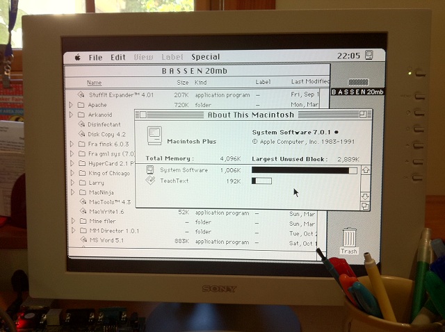
I’ve made some progress on Plus Too, but don’t get overly excited by the photo until you understand what it’s doing. I’ve finished the Verilog implementation of the video timing and pixel shifting modules, as well as some portions of the address decoder and the interleaved memory controller that I described earlier. I synthesized those modules, added a fake 32K ROM implemented inside the FPGA, and mapped it into the portion of the address space where the screen buffer is supposed to reside. I filled the ROM with a random 512 x 342 Mac desktop screenshot that I grabbed from the web. Using my Spartan 3A development board, I downloaded this design to the FPGA, and connected a standard VGA monitor. The result is the photo you see here. It’s just a static image, and there’s no interactivity, no software, and no CPU.
So what does this prove? Not too much yet, but it demonstrates that my video timing module generates the correct memory addresses and load enable signals, and with the correct timing. It also demonstrates that my pixel shifter module retrieves data from memory correctly, using the unconventional “double pumping” technique that was described in the memory controller blog entry. This technique performs two 16-bit wide loads every eight cycles of 8 MHz CPU clock, on the 5th and 7th cycle. Because the intervals between loads aren’t constant, the pixel shifter module must load the data into a different portion of the shift register for 5th cycle loads vs 7th cycle loads.
Long story short: some encouraging pictures to look at while I continue to work on the meat of the design for my Mac Plus clone.
Be the first to comment!Too Many Pins!
The primary components for Plus Too will be the 68000 CPU, RAM, ROM, maybe a microcontroller, and an FPGA containing all the simulated hardware and glue logic. For the FPGA, I’ve been doing some rough estimation of the number of I/O pins and logic resources needed, and it’s a lot! The I/O count looks like it will be at least 117 pins, and that doesn’t even include any allowance for FPGA to microcontroller communication. Because so many of an FPGA’s pins are consumed by power connections and other fixed-purpose stuff, to get 117 user I/Os it looks like I’ll need a device with at least 208 physical pins. Ugh. I’m definitely not comfortable with the idea of soldering that. The 100-pin TQFP in Tiny CPU was bad enough.
Here’s a quick breakdown of how to get to 117 pins:
- 40 – for the CPU address and data bus
- 14 – for other CPU connections like the address strobes, interrupt lines, function code, /DTACK
- 22 – for the address output of the video circuitry (could possibly be reduced to 15)
- 16 – for the parallel load input of the video shift register
- 7 – various select, enable, and output signals
- 4 – keyboard and mouse connections
- 4 – configuration of simulated RAM and ROM size
- 3 – video hsync, vsync, and data
- 5 – other
As I type this, I can already think of a few other signals I forgot, and I’m almost certainly going to need a wide connection between the FPGA and microcontroller too. The final number of I/Os could be in the 140-150 range, forcing me into an even scarier 240-pin QFP package, or the hobbyist’s nightmare BGA package. That’s not good.
While it’s incredibly convenient to lump everything into one giant FPGA that can be reconfigured at will, the huge number of I/Os may force me to split out some functional units separately. The work could be divided across two or more smaller FPGAs, or a single FPGA plus a few well-chosen ICs like bus drivers that need lots of pins but little internal logic. Splitting things up may not be easy, though. In a lot of cases, I’d just end up with two ICs that needed an I/O connection to a signal instead of one, making matters even worse. Only where two wholly unrelated functional modules share the same FPGA could they be split without causing a lot of signal duplication. Splitting things up into more ICs will also result in a larger board, and a bigger PCB routing challenge. I’m definitely beginning to appreciate the difference between a design for a little 8-bit system like Tiny CPU vs a system with multiple 24-bit address and 16-bit data busses.
EDIT: It also looks as if all the candidate FPGAs require a 1.2V supply. Given that I already need 3.3V and 5V for other components in the system, that means I’ll need a three-voltage design. Yuck, yuck, yuck.
Read 7 comments and join the conversationPlus Too Keyboard and Mouse
Digging further into the Plus Too design details, the next systems to consider are the keyboard and mouse. I plan to use a PS2-type keyboard and mouse, since they both communicate with a fairly simple serial protocol that’s easy to work with. The downside of PS2 input devices is that they’re growing less common, having been mostly replaced with USB devices now. They also require a 5V power supply, whereas everything else in the Plus Too will run at 3.3V. Perhaps a future version of the Plus Too might add USB input support with a microcontroller serving as a USB host, but for now PS2 is it.
PS2 Mouse
A standard PS2 mouse uses a bidirectional serial interface to communicate with the computer. The details of arbitrating control of the clock and data lines to determine the direction of a transfer make the interface more complex than a one-way serial connection, but there are many good examples found online that explain the process well. When power is first applied, the mouse enters a passive state. The first thing the computer must do is send the mouse a command instructing it to enter “stream mode”, which is accomplished by sending the command byte $F4. The mouse acknowledges the command by sending the byte $FE.
Once the mouse enters stream mode, it will send a 3-byte update packet to the computer whenever the mouse position or button state change. This packet contains the current state of the left, middle, and right mouse buttons, as well as two 9-bit signed values indicating how far the mouse has moved in X and Y since the last packet. The mouse only reports these movement deltas, not its current position in absolute terms. A delta of 1 unit in X or Y represents a physical movement of about 1/4 of a millimeter.
Chapter 10 of the book FPGA Prototyping by Verilog Examples is entirely devoted to the development of a PS2 mouse interface, freeing me from the need to write one myself.
Mac Plus Mouse
The Mac Plus mouse operates differently from a PS2 mouse. The Plus mouse is a dumb device with five wires connected to it: one to the mouse button, and four others connected to rotary quadrature encoders for the mouse ball (two for the X axis and two for the Y axis). The quadrature encoder lines send square wave trains to the Mac that change with the velocity and direction of the mouse. These quadrature signals are interpreted by the OS software to determine mouse movement deltas, and ultimately mouse position.
This presents a problem, because the PS2 mouse operates one level of abstraction above the Plus mouse. Quadrature encoded data is not available from the PS2 mouse, and so can’t be provided to the Mac OS running on the Plus Too hardware.
Mouse Hardware Simulation
One solution would be to generate fake quadrature data in the FPGA, based on the movement deltas reported by the PS2 mouse. If the Ps2 mouse reported a movement of +3 on the X axis, the FPGA would need to synthesize 3 cycles of quadrature square waves, with the appropriate phase relationships between the 4 quadrature signals to indicate positive X axis movement. This would also require simulating the portions of the Mac’s VIA and SCC serial controller to which the mouse signals are connected. One quadrature signal on each axis triggers an SCC interrupt, which is 68000 interrupt #2. Any state change for these signals will trigger an interrupt. The remaining quadrature signals and the mouse button are sampled passively through the VIA on port B. State changes for these signals will not trigger an interrupt, but they are tested inside the mouse interrupt handler (quadrature signals) and VBLANK interrupt handler (mouse button).
Mouse Cheating
While direct simulation of the mouse hardware should work, it could be tedious to implement, especially considering the simulation of VIA and SCC behavior needed. An alternative solution is to make use of knowledge about the Mac OS, and directly poke mouse bytes into the location in memory where the mouse driver would normally store them. In the case of the classic Mac OS, the low memory global MTemp at location $000828 stores the position from the most recent mouse interrupt. The FPGA address decoder could be modified to create a “hole” in RAM at this address, so that it was actually implemented as a register in the FPGA. When the OS software went to fetch the mouse position from memory, it would actually get it from the PS2 interface circuit in the FPGA. The mouse interrupt would never be invoked, yet the position of the mouse would still magically continue to be tracked by the OS. This would free me from having to worry about quadrature signals, or simulating any mouse-related VIA or SCC behavior.
This solution seems a bit questionable, but it’s the method used by at least one popular Mac emulator, and is reportedly compatible with virtually all Mac software. I will probably use this solution, at least at first. The drawback is that it’s not a true replica of the actual Mac hardware, but a software-level cheat. If someone discovered a new version of Mac OS that worked differently or stored the mouse position at a different memory location, then this solution wouldn’t work. It’s possible that a real-world alternative OS (Unix for Mac 68K?) might not work with this solution either. But since the locations of the relevant low memory globals are hard-coded in ROM, any hypothetical incompatible OS or program would have to go to the length of patching the ROM mouse driver and replacing it with a custom, incompatible one. That seems very unlikely, so I think it’s safe to rely on this solution.
PS2 Keyboard
A PS2 keyboard uses a similar serial connection to a mouse. Technically it’s a bidirectional connection, but in practice there’s no need to send anything to the keyboard, so it can be implemented as a one-way serial connection. When a key is pressed, the keyboard immediately sends a “make” scan code. When a key is released, the keyboard sends another “break” scan code. What makes things challenging is that scan codes are variable length, have no obvious correlation to keys that were pressed, and have no consistent correlation between make and break codes for the same key. Keeping track of it all requires a state machine and a scan code translation table. FPGA Prototyping by Verilog Examples chapter 9 describes the design of a PS2 keyboard interface.
Mac Plus Keyboard
The Mac Plus keyboard operates somewhat differently. It uses a bidirectional connection, and the keyboard only transmits keypress information when explicitly instructed to by the Mac. The Mac OS sends an “Inquiry” command to the keyboard every 1/4 second. If the keyboard has any keypress data in its internal buffer, it immediately returns it. If the buffer is empty, and no keys are pressed within the next 1/2 second, the keyboard responds with a NULL keypress.
The keyboard protocol also defines an “Instant” command that omits the 1/2 second timeout, as well as a “Model Number” query and a command to trigger a self-test. All of these will need to be simulated, since the Mac OS ROM routines use them all.
Plus keyboard scan codes are somewhat more sensible than for PS2 keyboards. All scan codes are a single byte. Bit 7 distinguishes between key-down and key-up events, and bits 6-1 indicate the specific key. Bit 0 is not used and is always set to 1.
The physical connection to the Mac keyboard uses a bidirectional serial connection very similar to the PS2 keyboard.
Plus Too Keyboard
The Plus Too keyboard module will need state machines to handle both the PS2 and the Mac interfaces, as well as tables for both sets of scan codes to facilitate translation between them. It will also need an internal buffer to hold scan codes received from the PS2 side until the next 1/4 second interval when an “Inquiry” command is received.
Some PS2 keyboard keys have no Mac equivalent (function keys, Home, etc). These will need to be silently thrown away by the keyboard module.
The Mac OS implements key repeating in software. If enough time elapses after a KeyDown without a corresponding KeyUp, the OS begins to generate additional virtual keypresses of the same key. In contrast, key repeating is performed in hardware by a PS2 keyboard, and the repeats are sent as additional “make” scan codes. The Plus Too keyboard module will need to suppress these, by keeping track of which keys are currently pressed down, and ignoring any further make codes for those keys.
Although the real Mac hardware uses a serial connection to communicate with the keyboard, at the OS level all keyboard communication is performed byte-by-byte, using a register in the VIA. When a full byte has been received from the keyboard, the VIA signals the “data ready” interrupt, and an OS routine fetches the byte from a memory-mapped location. This is convenient, because it means the Plus Too keyboard module can work at the byte level, by responding to read/write requests at the appropriate memory-mapped locations, and won’t need to simulate the details of the serial connection.
Read 2 comments and join the conversation