

RC Servo Signal Decoder, Part 2
It works! I’ve continued poking away at this circuit to decode an RC airplane servo signal and trigger a camera shutter during flight, and I’m happy to report success!Once I switched to using the CD4013 flip-flop with a positive logic clear input instead of negative logic, it was a piece of cake. I have to say, living just a mile from one of the USA’s largest electronics dealers (Jameco) is pretty sweet. I can hit their web site and place an order for practically any obscure electronic component I can think of, then cruise down to their offices and pick it up from the will-call desk an hour later. Nice!I rebuilt the decoder circuit that I discussed last time, soldering everything together “dead bug” style. This was necessary in order to keep everything as small as possible, so I could fit it inside the camera body. I forgot to take a photo before I closed everything up, but it looks very similar to this example from laureanno.com: When I first connected the servo, decoder, and camera, it didn’t work. Nothing happened when I toggled the switch on my RC transmitter. Setting up the oscilloscope again, I was able to see that the reference pulse width generated by the RC circuit I’d built was about twice as long as it should have been. I’m not sure how that happened, even with 20% tolerance components, but I was able to quickly swap in a different value resistor, and get it working perfectly. Then with a bit of creative packing, I managed to cram it all back inside the camera body.Today during my lunch hour, I was able to try it out for the first time. The shutter trigger worked fabulously! I wish I could say the same for the quality of the pictures, but unfortunately the focus wasn’t set quite right, and the photos are a little blurry. They’re still pretty fun to look at though. I was flying next to the headquarters of Oracle Corporation in Redwood City, California. Those are the clustered cylinder-shaped mirrored buildings you see in the photos. The plane looks like it was a little higher than the tallest building, which I think is 20 stories tall. See if you can find me in some of the photos!Click any of the thumbnails below to see the full-sized version.


 February 27 Edit: I corrected the focus problem, and tried again. Unfortunately I got the propeller in some of the shots, and this new set wasn’t from as high an altitude. But I did get some great shots of the bay, an aerial self-portrait, and a flock of Canada geese.


RC Servo Signal Decoder for Camera Shutter Switch
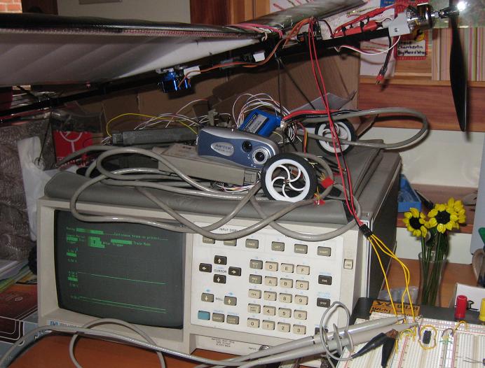
Hey, I’m back. I think my oscilloscope made me do it. For the past six months I’ve been working with RC airplanes, not doing any electronics work. The oscilloscope has been taking up space on my desk while it sits untouched, gathering dust. Last week I finally decided I was never going to use it again, and packed it away in a closet. But that got me to thinking about electronics again, and about what kind of projects I could do related to RC. So after just a few days, the oscilloscope has returned from its closet banishment and is in use once more for a new project.
I recently bought an Aiptek SD 1.3 megapixel camera, with the idea to mount it on the fuselage of one of my planes, and do some aerial photography. The Aiptek weighs just 52 grams (about 2 ounces), and so it won’t weigh down the plane excessively. But the tricky part is finding a way to activate the shutter while the plane is in the air. It turns out that this is mostly a solved problem, and it’s possible to build a circuit to decode the servo signal from an unused receiver channel, creating a 0 or 1 pulse depending on the position of a transmitter switch or stick. Then by hacking into the camera guts and a bit of soldering, that pulse can be used to trigger the shutter.
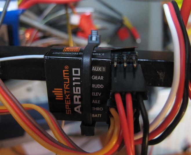
Here’s one of my planes (a GWS Slow Stick), with three spare wires hooked into the receiver’s “gear” channel (which I don’t normally use), connected to the oscilloscope and a growing circuit on the protoboard. It turns out that these servo signals for the channels are ideal for hacking with digital logic. Of the three wires connected to the receiver, one is ground, one is a regulated +5 volts, and one is a modulated position signal that indicates the desired position for that channel (rudder, elevator, aileron, flaps, gear, whatever). The connectors are even standard 0.1 inch male headers. What could be easier?
I examined the servo signal with the oscilloscope. It’s a regular pulse train with a 22ms period. The width of the pulse varies depending on the desired position for the channel. The width is about 1.2ms at the minimum position, and 2ms at the maximum position. Taking 1.6ms as the midpoint, what’s needed is a circuit that outputs 0 if the pulse width is less than 1.6ms, and 1 if it’s greater than 1.6ms. This could be done many different ways: the first two that come to mind are a small microcontroller, or a low-pass filter that turns the servo signal into a DC voltage, and compares it to a reference voltage.
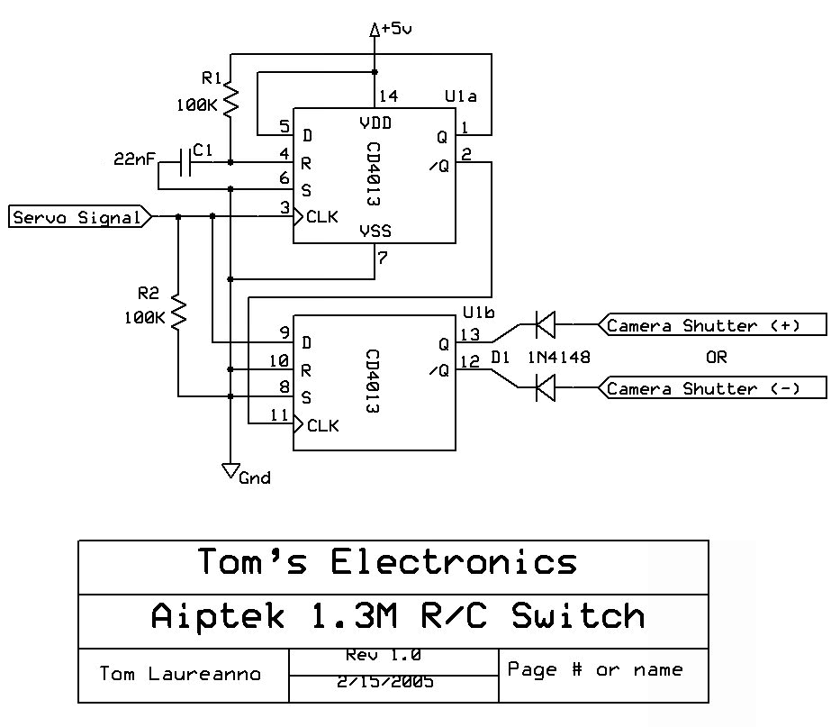
I’ve decided to follow another example I found, which I thought was especially clever. It uses just two flip-flops and a couple of passive components. You can check out the circuit schematic for the details. The servo signal pulse train is used to clock the first flip-flop. It’s D input is tied high. When it’s clocked, its Q output goes high, which begins to charge an RC circuit. When the capacitor voltage gets high enough, it activates the asynchronous reset, clearing the Q output. The complementary /Q output is used to clock the second flip-flop, whose D input is the servo signal. If the RC time constant is chosen correctly, then the second flip-flop will be clocked 1.6ms after the first one, sampling the servo signal at that time. If the pulse width is less than 1.6ms it will sample a 0, otherwise it will sample a 1. Pretty neat!
My only headache is that I don’t have the 4013 CMOS flip-flop called for in the circuit. I do have lots of 74LS74 flip-flops, which are similar, but are TTL designs with an active low asynchronous reset instead of active high. I’d thought it would be simple to modify the circuit to work with an active low reset, but after a couple of hours of futzing around with it, I concluded that it’s either not possible, or I’m just not smart enough. I started by swapping the positions of the resistor and capacitor, but the circuit initializes in the reset state and never exits it. And even if I found a solution to that, the input current on this LS series chip is so high, that with a 10K resistor to ground, the voltage at the input pin is actually pulled up to 2 volts! Ack! I decided I’ll just buy a 4013 for a few cents, and stop banging my head.
Read 5 comments and join the conversationFail
 OK, it’s time to admit defeat. 3D Graphics Thingy is not going to happen. It’s been six months since I worked on it. Heck, I even let my web hosting account expire due to neglect.
So what happened? I ran hard into the memory interface wall. Getting a decent DRAM controller working proved to be far, far more difficult than I’d expected, even with the assistance of Xilinx wizards and prebuilt controller packages. And since getting a working memory interface is a precondition to actually doing any of the 3D stuff, well, that sure put a damper on things.
A second reason for failure is that I found working with FPGAs to be abstract and unsatisfying, and the tool software to be a nightmare. When I built BMOW, I was constantly wiring things, debugging with the oscilloscope, buying new chips, soldering switches, and generally being hands-on. In contrast, 3DGT development ended up being nothing but writing Verilog in a text editor, and wondering why the Xilinx synthesis tools never did what I expected them to. The FPGA hardware itself just sat, untouched.
So what’s next? Since last summer, I haven’t done any electronics work at all, except building a light saber from a string of Christmas lights and a flourescent tube cover. I’ve gotten pretty involved in remote control vehicles, primarily RC planes, which give a few excuses to solder and build simple circuits. I have half an idea to use an Arduino with my Slow Stick somehow, to collect acceleration data in flight, or automate aerial photography or something.
Maybe I’ll come back to the CPU design thing again at some point. I still have a 68008 and some other parts I bought last year that I never got to use, so those are still waiting for me. For all those who contacted me asking if they could build something like BMOW or 3DGT, or asking for advice, send me a note and let me know how your projects are progressing now.
Happy hacking wishes to you all!
Read 8 comments and join the conversationSDRAM
I think I’m making life more difficult than it needs to be, trying to get this DDR2 SDRAM interface to work. It’s not that the logical interface is so complicated, really… you set your row and column addresses, do a burst transaction, check for refresh… not trivial, but not rocket science either. And the Xilinx MIG or other vendor-specific wizard will generate a memory interface for you to use as a starting point.No, what seems to be difficult is that the margin for error with DDR2 SDRAM is much smaller than with SRAM or plain (single data rate) SDRAM. The voltages are lower, the timing tolerances are tighter, and much more care must be given to compensating for things like possible skew, processes variation between different FPGAs, power supply tolerances, and a host of other worries.I’ve been reading a LOT on this topic in the past couple of weeks, and I’ve been struck by one thing. Except for my Xilinx Spartan 3A starter board, and Altera’s comperable Cyclone III board, I’ve seen zero boards that use DDR or DDR2 memory. The all use plain SDR SDRAM, also known as PC100 or PC133 depending on the speed. I looked at boards in the $150 to $300 range from Opal Kelly, KNJN, XESS, and others, and they all use plain SDR SDRAM. Maybe I should take a hint?Meanwhile, I’ve been digesting as much FPGA documentation as I can. So far I’ve chewed through about 1500 pages of the Xilinx MIG user manual, Spartan 3 series user manual, and Spartan 3A addendum, and I’m midway through the comprehensive book FPGA Prototyping by Verilog Examples: Xilinx Spartan-3 Version. It’s the best “getting started” reference I’ve seen yet, with good coverage of Verilog, FPGA hardware, and the Xilinx software tools.
Read 10 comments and join the conversationSmall Progress
 Finally, some small progress on the memory interface. After banging my head every which way against the Xilinx tools, and reading everything I could find on the subject, I came across Leo Silvestri’s page on modifying the Xilinx MIG memory controller design for a Spartan 3E board. It’s for a different kit and an older version of the software, but with his help I was finally able to build the reference design and testbench for the Spartan 3A board, program it to the FPGA, and see the LED that indicates success. It’s not very exciting, but it’s progress.I still can’t believe all the steps I went through, and the whole process has made me quite bitter about Xilinx’s software tools. I’m sure it would be easier if I had better general knowledge of this field, but the last few weeks of this project have been like being lost at sea, and totally disoriented. It still feels more like a series of disconnected guesses than a genuine understanding, but here’s what I’ve managed to piece together on the topic of using the DDR2 SDRAM that’s on the Spartan 3A kit board.
- The Xilinx MIG can’t be used to generate a new memory controller design for the Spartan 3A board. This is because the way the SDRAM on the board is connected to the FPGA pins violates some of the MIG design rules. The only solution is to use the pre-built Spartan 3A board reference controller design, which then locks you into a specific burst length and CAS latency, or to hand-modify the code generated by the MIG, which is way beyond the skills of a noob like me.
- Using the newest version of the Xilinx ISE and MIG, attempting to add the Spartan 3A reference design to your project will cause a crash. No answer from Xilinx support on this.
- You can also get the Spartan 3A reference design as a zip file. But if you unzip it, add all the files to a new ISE project, and try to build it, you’ll get lots of errors about non-existant nets that I couldn’t resolve.
- There’s also a batch file in the zip file that will create a new ISE project for you. But try to build it, and you’ll be told that the design requires a ChipScopePro license, which is Xilinx’s software logic analyzer. I found a discussion of this on the Xilinx forums, but no resolution other than to create a new controller design that omits ChipScopePro support, which is impossible for this board due to issue number 1 above.
- What finally worked was to hand-edit the reference design, deleting parts of it semi-randomly until the ChipScopePro error disappeared. It turned out that required removing three modules called icon, ila, and vio, none of which seemed obviously related to debugging to me.
So there you have it. The next step will be to begin to actually use this interface for something more interesting than lighting up an LED. I’m just now realizing that the interface created by the MIG is just the first, small step towards what the 3DGT memory controller must eventually become. It’s not enough to simply have an interface that permits reading and writing. To achieve half-way decent performance, much care will be required to manage and coordinate those reads and writes, minimizing waiting and wasted time, and maximizing throughput. And to top it off, it’s going to need a bus master to arbitrate memory access between the display circuit, pixel processors, vertex processors, and any other consumers of memory. All this is a substantial project in itself, that will need to be at least partially completed before any real progress can begin on the 3D part of 3DGT. Looks like a long, slow climb, but I’m moving ahead.
Read 4 comments and join the conversationXilinx Memory Controller
I think I’m about ready to crush this Xilinx starter kit under my boot, and use the pulverized component dust to scrub my toilet. That’s not quite fair, though, as my frustration isn’t really with the hardware, but with the inexplicable Xilinx software. At this point, I’ve spent about 20 hours over a couple of weeks, just trying to instantiate the sample Xilinx SDRAM memory controller. I’m amazed that something so central to the use of a Xilinx FPGA or starter kit could be so obtuse. Or maybe it’s me that’s obtuse, but regardless, I was never so exasperated in all the time I was working on BMOW. Back then, at least each piece of hardware was small and understandable, and any errors were of my own making. Now I’m spending hour upon hour attempting to decode the error messages from Xilinx’s software, and trying to guess at how they intended this process to work. I expected something like:
- Create new project
- Run “memory interface generator” wizard (which Xilinx calls the M.I.G.)
- Choose memory type, speed, etc.
- The wizard adds some auto-generated .v and .ucf (user constraints) files to my project
- Optionally, wizard also adds a test bench, or some kind of example
- Synthesize the example, program it to the starter kit, and blink some LEDs to show that it worked.
That was the theory anyway. The reality has been a long series of software errors and omissions too dull to recount in detail. The short version is that when I use the MIG to generate an interface specifically for the Spartan 3A starter kit, the MIG crashes. If I follow some hazy instructions for manually adding the reference design to the project without using the MIG, then I get something that fails the “translate” step. If I use the MIG to generate a new interface design for a board that just happens to have the same hardware as the Spartan 3A starter kit, I also get something that fails the “translate” step. In either case, before the fatal errors, there are many warnings saying that dozens of flip-flops were determined to have a constant 0 or 1 value, and so were optimized away, as well as copious other warnings. Clearly I’m doing something very wrong, but creating a sample design using the reference memory interface on the reference board seems like it should be about as simple a case as it’s possible to get.
I would have given up on it a while ago, except that with no memory interface, there can be no 3D Graphics Thingy. This simply must be made to work in order for the project to progress any further. Unfortunately I’m about out of ideas. I need to find a simple walk-through tutorial that starts with “open ISE, press the New Project button” and finishes with happy green checkmarks next to all the steps in the processes window for an example design using the MIG controller. There are only about 10 mouse clicks needed between that start and finish, so it would seem hard to mess it up much. Either I’m doing something basic wrong, or omitting something, or my computer is haunted. With luck, it will become clear tomorrow.
Read 8 comments and join the conversation